- 您現(xiàn)在的位置:買賣IC網(wǎng) > PDF目錄382710 > U635H64D1K45G1 PowerStore 8K x 8 nvSRAM PDF資料下載
參數(shù)資料
| 型號(hào): | U635H64D1K45G1 |
| 英文描述: | PowerStore 8K x 8 nvSRAM |
| 中文描述: | PowerStore 8K的× 8非易失 |
| 文件頁數(shù): | 2/14頁 |
| 文件大?。?/td> | 149K |
| 代理商: | U635H64D1K45G1 |

U635H64
2
March 31, 2006
STK Control #ML0052
Rev 1.0
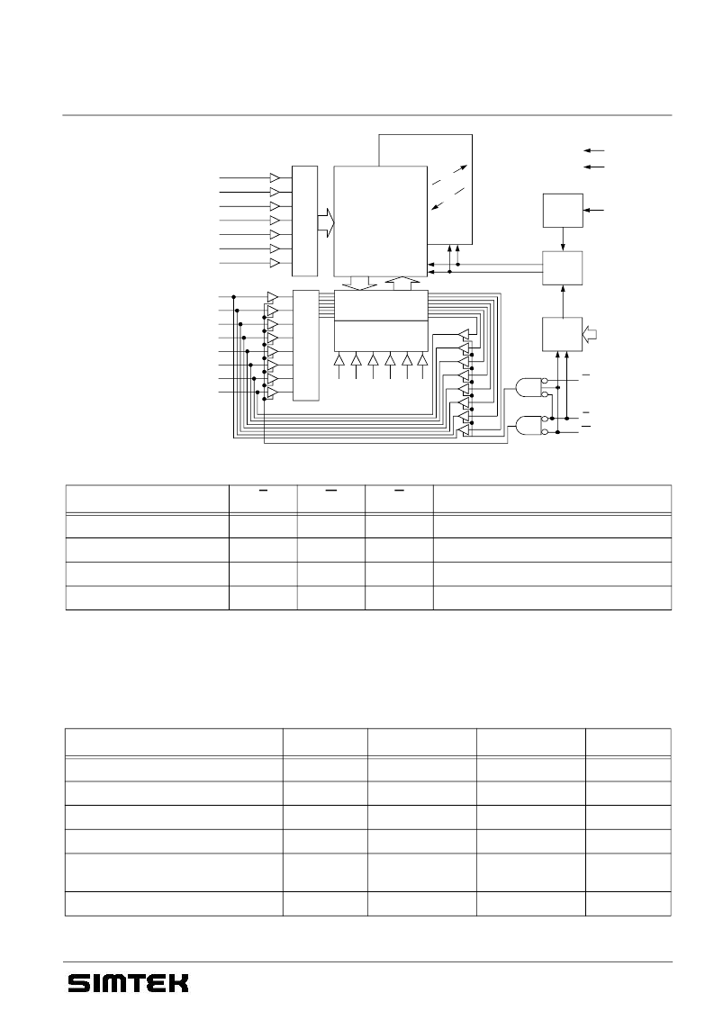
Block Diagram
Operating Mode
E
W
G
DQ0 - DQ7
Standby/not selected
H
*
*
High-Z
Internal Read
L
H
H
High-Z
Read
L
H
L
Data Outputs Low-Z
Write
L
L
*
Data Inputs High-Z
Truth Table for SRAM Operations
a:
Stresses greater than those listed under Absolute Maximum Ratings“ may cause permanent damage to the device. This is a stress
rating only, and functional operation of the device at condition above those indicated in the operational sections of this specification is
not implied. Exposure to absolute maximum rating conditions for extended periods may affect reliability.
Absolute Maximum Ratings
a
Symbol
Min.
Max.
Unit
Power Supply Voltage
V
CC
-0.5
7
V
Input Voltage
V
I
-0.3
V
CC
+0.5
V
Output Voltage
V
O
-0.3
V
CC
+0.5
V
Power Dissipation
P
D
1
W
Operating Temperature
C-Type
K-Type
T
a
0
-40
70
85
°
C
°
C
Storage Temperature
T
stg
-65
150
°
C
Characteristics
All voltages are referenced to V
SS
= 0 V (ground).
All characteristics are valid in the power supply voltage range and in the operating temperature range specified.
Dynamic measurements are based on a rise and fall time of
≤
5 ns, measured between 10 % and 90 % of V
I
, as well as
input levels of V
IL
= 0 V and V
IH
= 3 V. The timing reference level of all input and output signals is 1.5 V,
with the exception of the t
dis
-times and t
en
-times, in which cases transition is measured
±
200 mV from steady-state voltage.
*
H or L
EEPROM Array
128 x (64 x 8)
STORE
RECALL
SRAM
Array
128 Rows x
64 x 8 Columns
A5
A6
A7
A8
A9
A11
A12
A0 - A12
Store/
Recall
Control
R
V
CC
V
SS
G
E
W
Software
Detect
Power
Control
V
CC
DQ0
DQ1
DQ2
DQ3
DQ4
DQ5
DQ6
DQ7
Column I/O
Column Decoder
A0 A1
A2 A3 A4A10
I
相關(guān)PDF資料 |
PDF描述 |
|---|---|
| U635H64S2C25 | PowerStore 8K x 8 nvSRAM |
| U635H64S2C25G1 | PowerStore 8K x 8 nvSRAM |
| U635H64S2C35 | PowerStore 8K x 8 nvSRAM |
| U635H64S2C35G1 | PowerStore 8K x 8 nvSRAM |
| U635H64S2C45 | PowerStore 8K x 8 nvSRAM |
相關(guān)代理商/技術(shù)參數(shù) |
參數(shù)描述 |
|---|---|
| U635H64DC25 | 制造商:未知廠家 制造商全稱:未知廠家 功能描述:NVRAM (EEPROM Based) |
| U635H64DC35 | 制造商:未知廠家 制造商全稱:未知廠家 功能描述:NVRAM (EEPROM Based) |
| U635H64DC45 | 制造商:未知廠家 制造商全稱:未知廠家 功能描述:NVRAM (EEPROM Based) |
| U635H64DK25 | 制造商:未知廠家 制造商全稱:未知廠家 功能描述:NVRAM (EEPROM Based) |
| U635H64DK35 | 制造商:未知廠家 制造商全稱:未知廠家 功能描述:NVRAM (EEPROM Based) |
發(fā)布緊急采購,3分鐘左右您將得到回復(fù)。