- 您現(xiàn)在的位置:買賣IC網(wǎng) > PDF目錄382703 > U4083 Low-Power Audio Amplifier for Telephone Applications PDF資料下載
參數(shù)資料
| 型號: | U4083 |
| 元件分類: | 運動控制電子 |
| 英文描述: | Low-Power Audio Amplifier for Telephone Applications |
| 中文描述: | 低功耗音頻放大器電話應(yīng)用 |
| 文件頁數(shù): | 3/11頁 |
| 文件大小: | 132K |
| 代理商: | U4083 |

U4083B
Preliminary Information
TELEFUNKEN Semiconductors
Rev. A2, 07-Apr-97
3 (11)
Pin 6: Supply and power dissipation
Power dissipation is shown in figures 8 to 10 for different
loads. Distortion characteristics are given in figures 11 to
13.
P
totmax
T
jmax
– T
amb
R
thJA
where
T
jmax
= Junction temperature = 140
°
C
T
amb
= Ambient temperature
R
thJA
= Thermal resistance, junction-ambient
Power dissipated within the IC in a given application is
found from the following equation:
P
tot
= (V
S
I
S
) + (I
RMS
V
S
) – (R
L
I
RMS2
)
I
S
is obtained from figures 15
I
RMS
is the RMS current at the load R
L.
Operating range of the integrated circuit is defined with
a peak operating load current of
13). It is further specified with respect to different loads
in figure 14. The left (ascending) portion of each of the
three curves is defined by the power level at which 10%
distortion occurs. The center flat portion of each curve is
defined by the maximum output current capability of the
integrated circuit. The right (descending) portion of each
curve is defined by the maximum internal power dissipa-
tion of the IC at 25
°
C. At higher ambient temperatures,
the maximum load power must be reduced according to
the above mentioned equation.
Layout Considerations
200 mA (figures 8 to
Normally a snubber is not needed at the output of the IC,
unlike many other audio amplifiers. However, the PC
board layout, stray capacitances, and the manner in which
the speaker wires are configured, may dictate otherwise.
Generally the speaker wires should be twisted tightly, and
be not more than a few cm (or inches) in length.
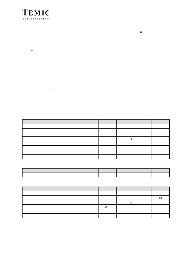
Absolute Maximum Ratings
Reference point Pin 7, T
amb
= 25
°
C unless otherwise specified.
Parameters
Symbol
V
S
Value
Unit
V
V
V
mA
°
C
°
C
°
C
mW
Supply voltage
Voltages
Disabled
Output current
Junction temperature
Storage temperature range
Ambient temperature range
Power dissipation: T
amb
= 60
°
C
Thermal Resistance
Pin 6
Pins 1, 2, 3 and 4
Pins 5 and 8
Pins 5 and 8
–1.0 to +18
–1.0 to (VS +1.0)
–1.0 to (VS +1.0)
250
+140
–55 to +150
–20 to +70
440
T
j
T
stg
T
amb
P
tot
SO8
Parameters
Symbol
R
thJA
Value
180
Unit
K/W
Junction ambient
Operation Recommendation
SO8
Parameters
Symbol
V
S
R
L
I
L
G
V
CD
T
amb
Value
2 to 16
8.0 to 100
200
0 to 46
VS
–20 to +70
Unit
V
Supply voltage
Load impedance
Load current
Differential gain (5.0 kHz bandwidth)
Voltage @ CD Pin 1
Ambient temperature range
Pin 6
Pins 5 to 8
mA
dB
V
°
C
相關(guān)PDF資料 |
PDF描述 |
|---|---|
| U4083B | Low-Power Audio Amplifier for Telephone Applications |
| U4083B-AFP | Low-Power Audio Amplifier for Telephone Applications |
| U4083B-AFPG3 | Low-Power Audio Amplifier for Telephone Applications |
| U4084B-FL | LOW POWER QUAD VOLTAGE COMPARATOR |
| U4084B | Low-Voltage, Voice-Switched Circuit for Hands-Free Operation |
相關(guān)代理商/技術(shù)參數(shù) |
參數(shù)描述 |
|---|---|
| U4083B | 制造商:TEMIC 制造商全稱:TEMIC Semiconductors 功能描述:Low-Power Audio Amplifier for Telephone Applications |
| U4083B-AFP | 制造商:TEMIC 制造商全稱:TEMIC Semiconductors 功能描述:Low-Power Audio Amplifier for Telephone Applications |
| U4083B-AFPG3 | 制造商:Temic / Atmel Wireless and Microcontrollers 功能描述: |
| U4083B-MFPG3 | 制造商:Atmel Corporation 功能描述:TELECOM AUDIO AMP |
| U4083B-MFPG3Y | 功能描述:音頻放大器 COM.CORDED AUDIO AMP RoHS:否 制造商:STMicroelectronics 產(chǎn)品:General Purpose Audio Amplifiers 輸出類型:Digital 輸出功率: THD + 噪聲: 工作電源電壓:3.3 V 電源電流: 最大功率耗散: 最大工作溫度: 安裝風(fēng)格:SMD/SMT 封裝 / 箱體:TQFP-64 封裝:Reel |
發(fā)布緊急采購,3分鐘左右您將得到回復(fù)。