- 您現(xiàn)在的位置:買賣IC網(wǎng) > PDF目錄382703 > U4083 Low-Power Audio Amplifier for Telephone Applications PDF資料下載
參數(shù)資料
| 型號(hào): | U4083 |
| 元件分類: | 運(yùn)動(dòng)控制電子 |
| 英文描述: | Low-Power Audio Amplifier for Telephone Applications |
| 中文描述: | 低功耗音頻放大器電話應(yīng)用 |
| 文件頁(yè)數(shù): | 2/11頁(yè) |
| 文件大?。?/td> | 132K |
| 代理商: | U4083 |

U4083B
TELEFUNKEN Semiconductors
Rev. A2, 07-Apr-97
Preliminary Information
2 (11)
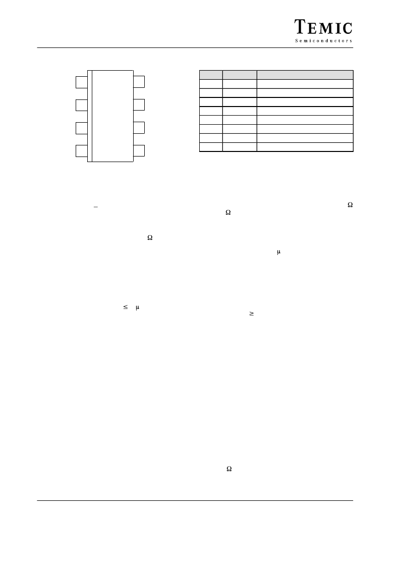
Pin Description
1
2
3
4
8
7
6
5
94 8022
Vi
FC1
FC2
GND
CD
VO1
VO2
VS
Figure 2. Pinning
Pin
1
2
3
4
5
6
7
8
Symbol
CD
FC2
FC1
V
i
VO1
V
S
GND
VO2
Function
Chip disable
Filtering, power supply rejection
Filtering, power supply rejection
Amplifier input
Amplifier output 1
Voltage supply
Ground
Amplifier output 2
Functional Description
Including External Circuitry
Pin 1: Chip disable
digital input (CD)
Pin 1 (chip disable) is used to power down the IC to con-
serve power or muting or both.
Input impedance at pin 1 is typically 90 k .
Logic 0 < 0.8 V
IC enabled (normal operation)
Logic 1 > 2 V
IC disabled
Figure 15 shows power supply current diagram. The
change in differential gain from normal operation to
muted operation (muting) is more than 70 dB.
Switching characteristics are as follows:
turn-on time
turn-off time
t
on
= 12 to 15 ms
t
off
2 s
They are independent of C
1
, C
2
and V
S
.
Voltages at Pins 2 and 3 are supplied from V
S
and there-
fore do not change when the U4083B is disabled.
Outputs– V
O1
(Pin 5) and V
O2
(Pin 8) –turn to a high im-
pedance condition by removing the signal from the
speaker.
When signals are applied from an external source to the
outputs (disabled), they must not exceed the range be-
tween the supply voltage, V
s
, and Ground.
Pins 2 and 3: Filtering, power supply rejection
Power supply rejection is provided by capacitors C
1
and
C
2
at Pin 3 and Pin 2, respectively. C
1
is dominant at high
frequencies whereas C
2
is dominant at low frequencies
(figures 4 to 7). Values of C
1
and C
2
depend on the
conditions of each application. For example, a line
powered speakerphone (telephone amplifier) will require
more filtering than a system powered by regulated power
supply.
The amount of rejection is a function of the capacitors and
the equivalent impedance looking into Pin 3 and Pin 2
(see electrical characteristic equivalent resistance, R).
Apart from filtering, capacitors C
1
and C
2
also influence
the turn-on time of the circuit at power-up since capaci-
tors are charged up through the internal resistors (50 k
and 125 k ) as shown in the block diagram.
Figure 1 shows turn-on time versus C
2
at V
S
= 6 V, for two
different C
1
values.
Turn-on time is 60% longer when V
S
= 3 V and 20%
shorter when V
S
= 9 V.
Turn-off time is less than 10 s
Pin 4: Amplifier input
Pin 5: Amplifier output 1 V
O1
Pin 8: Amplifier output 2 V
O2
V
i
There are two identical operational amplifiers. Amp.1 has
an open loop gain
80 dB at 100 Hz (figure 2), whereas
the closed loop gain is set by external resistors, Rf and Ri
(figure 3). The amplifier is unity gain stable, and has a
unity gain frequency of approximately 1.5 MHz. A closed
loop gain of 46 dB is recommended for a frequency range
of 300 to 3400 Hz (voice band). Amp.2 is internally set
to a gain of –1.0 (0 dB). The outputs of both amplifiers are
capable of sourcing and sinking a peak current of 200 mA.
Output voltage swing is between 0.4 V and V
s
– 1.3 V at
maximum current (figures 18 and 19).
The output dc offset voltage between Pins 5 and 8 (V
O1
– V
O2
) is mainly a function of the feedback resistor, R
f
,
because the input offset voltage of the two amplifiers
generally neutralize each other.
Bias current of Amp. 1 which is constant with respect to
V
s
, however flows out of Pin 4 (V
i
) and through R
f
,
forcing V
01
to shift negative by an amount equal to R
f
I
IB
and V
O2
positive to an equal amount.
The output offset voltage specified in the electrical char-
acteristics is measured with the feedback resistor
(R
f
= 75 k ) shown in typical application circuit. It takes
into account bias current as well as internal offset voltages
of the amplifiers.
相關(guān)PDF資料 |
PDF描述 |
|---|---|
| U4083B | Low-Power Audio Amplifier for Telephone Applications |
| U4083B-AFP | Low-Power Audio Amplifier for Telephone Applications |
| U4083B-AFPG3 | Low-Power Audio Amplifier for Telephone Applications |
| U4084B-FL | LOW POWER QUAD VOLTAGE COMPARATOR |
| U4084B | Low-Voltage, Voice-Switched Circuit for Hands-Free Operation |
相關(guān)代理商/技術(shù)參數(shù) |
參數(shù)描述 |
|---|---|
| U4083B | 制造商:TEMIC 制造商全稱:TEMIC Semiconductors 功能描述:Low-Power Audio Amplifier for Telephone Applications |
| U4083B-AFP | 制造商:TEMIC 制造商全稱:TEMIC Semiconductors 功能描述:Low-Power Audio Amplifier for Telephone Applications |
| U4083B-AFPG3 | 制造商:Temic / Atmel Wireless and Microcontrollers 功能描述: |
| U4083B-MFPG3 | 制造商:Atmel Corporation 功能描述:TELECOM AUDIO AMP |
| U4083B-MFPG3Y | 功能描述:音頻放大器 COM.CORDED AUDIO AMP RoHS:否 制造商:STMicroelectronics 產(chǎn)品:General Purpose Audio Amplifiers 輸出類型:Digital 輸出功率: THD + 噪聲: 工作電源電壓:3.3 V 電源電流: 最大功率耗散: 最大工作溫度: 安裝風(fēng)格:SMD/SMT 封裝 / 箱體:TQFP-64 封裝:Reel |
發(fā)布緊急采購(gòu),3分鐘左右您將得到回復(fù)。