- 您現(xiàn)在的位置:買賣IC網(wǎng) > PDF目錄366059 > TZA3031AHL (NXP SEMICONDUCTORS) SDH/SONET STM1/OC3 laser drivers(SDH/SONET STM1/OC3 激光驅(qū)動器) PDF資料下載
參數(shù)資料
| 型號: | TZA3031AHL |
| 廠商: | NXP SEMICONDUCTORS |
| 元件分類: | 其它接口 |
| 英文描述: | SDH/SONET STM1/OC3 laser drivers(SDH/SONET STM1/OC3 激光驅(qū)動器) |
| 中文描述: | SPECIALTY INTERFACE CIRCUIT, PQFP32 |
| 封裝: | 5 X 5 X 1.40 MM, PLASTIC, LQFP-32 |
| 文件頁數(shù): | 15/32頁 |
| 文件大?。?/td> | 137K |
| 代理商: | TZA3031AHL |
第1頁第2頁第3頁第4頁第5頁第6頁第7頁第8頁第9頁第10頁第11頁第12頁第13頁第14頁當(dāng)前第15頁第16頁第17頁第18頁第19頁第20頁第21頁第22頁第23頁第24頁第25頁第26頁第27頁第28頁第29頁第30頁第31頁第32頁

2000 Feb 22
15
Philips Semiconductors
Product specification
SDH/SONET STM1/OC3 laser drivers
TZA3031AHL; TZA3031BHL;
TZA3031U
Loop mode for TZA3031BHL
The loop mode allows the total system application to be
tested. It allows for uninhibited optical transmission
through the fibre front-end (from the MPD through the
transimpedance stage and the data and clock recovery
unit, to the laser driver and via the laser back to the fibre).
Note that the optical receiver used in conjunction with the
TZA3031BHL must have a loop mode output in order to
complete the test loop.
The loop mode is selected by a HIGH level on pin ENL.
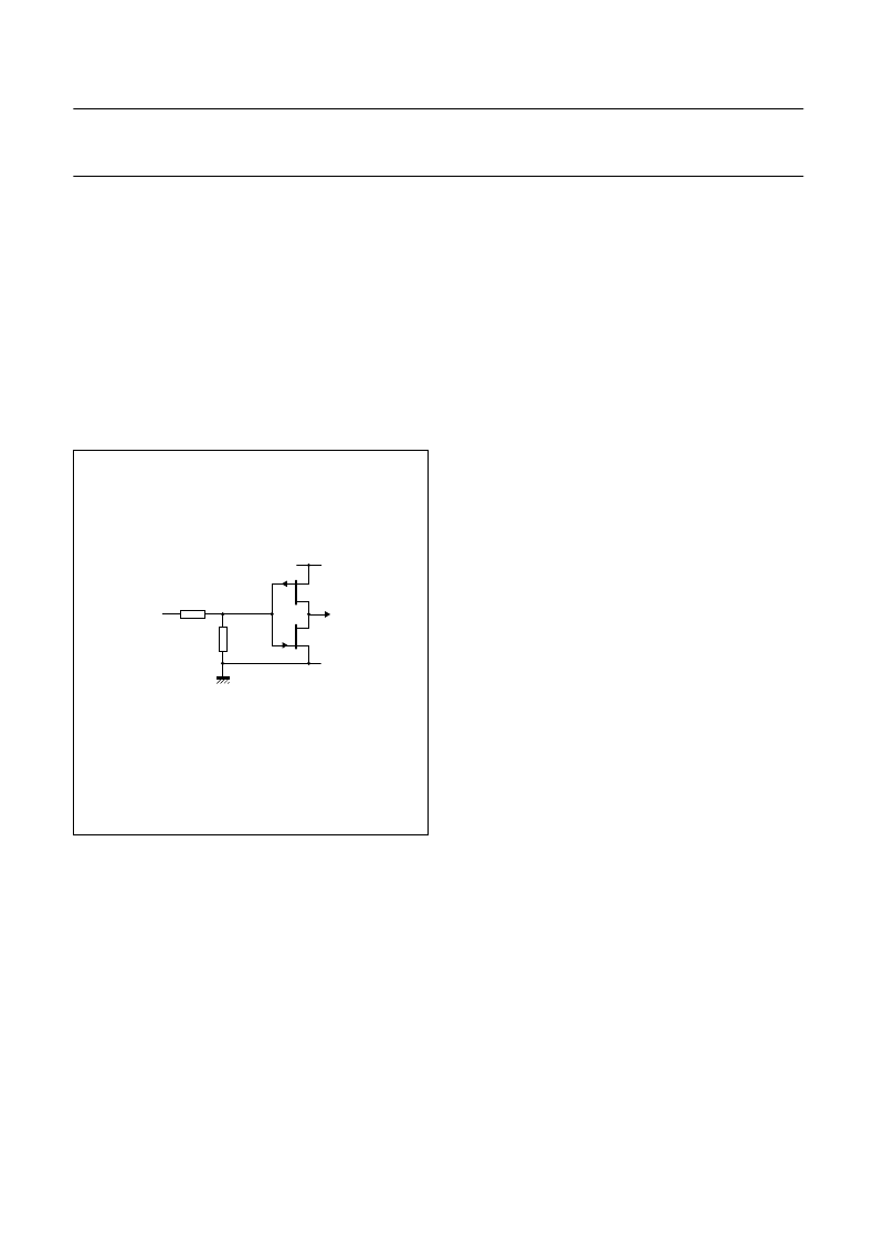
By default, pin ENL is pulled to a LOW level by a 25 k
pull-down resistor (see Fig.16).
Power supply connections
Refer to application diagrams Figs 18 and 19. Three
separate supply domains (labelled V
CC(G)
, V
CC(B)
, and
V
CC(R)
) provide isolation between the MPD current input,
the high-current outputs, and the PECL or CML inputs.
Each supply domain should be connected to a central V
CC
viaseparatefiltersasshownin Figs 18 and 19.
Allsupply
pins must be connected
. The voltage supply levels
should be equal to, and in accordance with, the values
specified in Chapter “Characteristics”.
To maximize power supply isolation, the cathode of the
MPD should be connected to V
CC(G)
and the anode of the
laser diode should be connected to V
CC(B)
. It is
recommended that the laser diode anode is also
connected to a separate decoupling capacitor C9.
Generally, the inverted laser modulation output (pin LAQ)
is not used. To correctly balance the output stage, an
equalization network (Z1) with an impedance comparable
to the laser diode is connected between pin LAQ and
V
CC(B)
.
All external components should be surface mounted
devices, preferably of size 0603 or smaller.
The components must be mounted as close to the IC as
possible.
It is especially recommended to mount the following
components very close to the IC:
Power supply decoupling capacitors C2, C3 and C4
Inputmatchingnetworkonpins DIN,DINQ,DLOOPand
DLOOPQ
Capacitor C5 on pin MONIN
Output matching network Z1 at the unused output
The laser.
Bare die ground
In addition to the separate V
CC
domains, the bare die
contains three corresponding ground (GND) domains.
Isolation between the GND domains is limited due to the
finite substrate conductance.
Mount the die preferably on a large and highly conductive
grounded die pad.
All GND pads must be bonded to the
die pad.
The external ground is thus ideally combined with
the die ground to avoid ground bounce problems.
Layout recommendations
Layout recommendations for the TZA3031AHL and
TZA3031BHL can be found in application note “AN98090
Fiber optic transceiverboard STM1/4/8, OC3,12,24,
FC/GE”
handbook, halfpage
MGS912
25 k
VCC(R)
GND
ENL
600
Fig.16 ENL input.
相關(guān)PDF資料 |
PDF描述 |
|---|---|
| TZA3034T | SDH/SONET STM1/OC3 postamplifiers |
| TZA3034 | SDH/SONET STM1/OC3 postamplifier |
| TZA3034TT | SDH/SONET STM1/OC3 postamplifier |
| TZA3034U | SDH/SONET STM1/OC3 postamplifier |
| TZA3041AHL | Gigabit Ethernet/Fibre Channel laser drivers(千兆位以太網(wǎng)/光纖通道激光驅(qū)動器) |
相關(guān)代理商/技術(shù)參數(shù) |
參數(shù)描述 |
|---|---|
| TZA3031BHL | 制造商:PHILIPS 制造商全稱:NXP Semiconductors 功能描述:SDH/SONET STM1/OC3 laser drivers |
| TZA3031U | 制造商:PHILIPS 制造商全稱:NXP Semiconductors 功能描述:SDH/SONET STM1/OC3 laser drivers |
| TZA3033 | 制造商:PHILIPS 制造商全稱:NXP Semiconductors 功能描述:SDH/SONET STM1/OC3 and STM4/OC12 transceiver |
| TZA3033T | 制造商:PHILIPS 制造商全稱:NXP Semiconductors 功能描述:SDH/SONET STM1/OC3 transimpedance amplifier |
| TZA3033U | 制造商:PHILIPS 制造商全稱:NXP Semiconductors 功能描述:SDH/SONET STM1/OC3 transimpedance amplifier |
發(fā)布緊急采購,3分鐘左右您將得到回復(fù)。