- 您現(xiàn)在的位置:買賣IC網(wǎng) > PDF目錄373724 > TSEV8388BFZA2 (Atmel Corp.) ADC 8-bit 1 GSPS PDF資料下載
參數(shù)資料
| 型號: | TSEV8388BFZA2 |
| 廠商: | Atmel Corp. |
| 元件分類: | ADC |
| 英文描述: | ADC 8-bit 1 GSPS |
| 中文描述: | ADC的8位1 GSPS的 |
| 文件頁數(shù): | 13/57頁 |
| 文件大小: | 1276K |
| 代理商: | TSEV8388BFZA2 |
第1頁第2頁第3頁第4頁第5頁第6頁第7頁第8頁第9頁第10頁第11頁第12頁當前第13頁第14頁第15頁第16頁第17頁第18頁第19頁第20頁第21頁第22頁第23頁第24頁第25頁第26頁第27頁第28頁第29頁第30頁第31頁第32頁第33頁第34頁第35頁第36頁第37頁第38頁第39頁第40頁第41頁第42頁第43頁第44頁第45頁第46頁第47頁第48頁第49頁第50頁第51頁第52頁第53頁第54頁第55頁第56頁第57頁
13
TS8388B
2144C–BDC–04/03
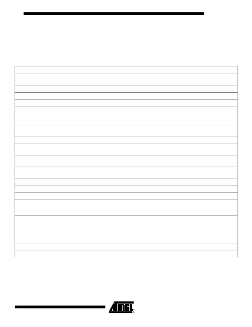
Package
Description
Pin Description
Note:
1. The common mode level of the output buffers is 1.2V below the positive digital supply.
For ECL compatibility the positive digital supply must be set at 0V (ground).
For LVDS compatibility (output common mode at +1.2V) the positive digital supply must be set at 2.4V.
If the subsequent LVDS circuitry can withstand a lower level for input common mode, it is recommended to lower the posi-
tive digital supply level in the same proportion in order to spare power dissipation.
Table 7.
TS8388BGL Pin Description (CBGA68 package)
Symbol
Pin number
Function
GND
A2, A5, B1, B5, B10, C2, D2, E1, E2, E11,
F1, F2, G11, K2, K3, K4, K5, K10, L2, L5
Ground pins.
To be connected to external ground plane.
V
CC
A4, A6, B2, B4, B6, H1, H2, L6, L7
+5V positive supply.
V
EE
A3, B3, G1, G2, J1, J2
5V analog negative supply.
DV
EE
F10, F11
-5V digital negative supply.
V
IN
L3
In phase (+) analog input signal of the Sample and Hold
differential preamplifier.
V
INB
L4
Inverted phase (-) of ECL clock input signal (CLK).
CLK
C1
In phase (+) ECL clock input signal. The analog input is
sampled and held on the rising edge of the CLK signal.
CLKB
D1
Inverted phase (-) of ECL clock input signal (CLK).
B0, B1, B2, B3, B4,
B5, B6, B7
A8, A9, A10, D10, H11, J11, K9, K8
In phase (+) digital outputs.
B0 is the LSB. B7 is the MSB.
B0B, B1B, B2B, B3B,
B4B, B5B, B6B, B7B
B7, B8, B9, C11, G10, H10, L10, L9
Inverted phase (-) digital outputs.
B0B is the inverted LSB. B7B is the inverted MSB.
OR
K7
In phase (+) Out of Range Bit. Out of Range is high on the
leading edge of code 0 and code 256.
ORB
L8
Inverted phase (+) Out of Range Bit (OR).
DR
E10
In phase (+) output of Data Ready Signal.
DRB
D11
Inverted phase (-) output of Data Ready Signal (DR).
GORB
A7
Gray or Binary select output format control pin.
- Binary output format if GORB is floating or V
CC
.
- Gray output format if GORB is connected at ground (0V).
GAIN
K6
ADC gain adjust pin. The gain pin is by default grounded, the
ADC gain transfer fuction is nominally close to one.
DIOD/DRRB
K1
Die function temperature measurement pin and
asynchronous data ready reset active low, single-ended ECL
input.
V
PLUSD
B11, C10, J10, K11
+2.4V for LVDS output levels otherwise to GND
(2)
.
NC
A1, A11, L1, L11
Not connected.
相關(guān)PDF資料 |
PDF描述 |
|---|---|
| TSEV8388BGL | ADC 8-bit 1 GSPS |
| TSEV8388BGLZA2 | ADC 8-bit 1 GSPS |
| TS8388BCFS | ADC 8-bit 1 GSPS |
| TS8388BCGL | ADC 8-bit 1 GSPS |
| TS8388BMF | ADC 8-bit 1 GSPS |
相關(guān)代理商/技術(shù)參數(shù) |
參數(shù)描述 |
|---|---|
| TSEV8388BGL | 制造商:e2v technologies 功能描述:ADC 8-BIT 1 GSPS BOARD - Trays |
| TSEV8388BGLZA2 | 制造商:e2v technologies 功能描述:TSEV8388BGLZA2 - Trays |
| TSEV86101G2BGL | 制造商:e2v technologies 功能描述:MUXDAC MUXDAC 10-BIT 1.2 GSPS - Trays |
| TSF-0.5-5 | 制造商:PMK 功能描述:SPRING TIP WITHOUT PLASTIC 0 5MM PK5 制造商:PMK 功能描述:SPRING TIP, WITHOUT PLASTIC 0, 5MM PK5 制造商:PMK 功能描述:SPRING TIP, WITHOUT PLASTIC 0, 5MM PK5; Accessory Type:Spring Tip; Body Diameter:0.5mm; Range:Check datasheet for delivery content! ;RoHS Compliant: NA |
| TSF-0.8-5 | 制造商:PMK 功能描述:SPRING TIP WITHOUT PLASTIC 0.8MM PCK 5 制造商:PMK 功能描述:SPRING TIP, WITHOUT PLASTIC 0.8MM PCK 5 制造商:PMK 功能描述:SPRING TIP, WITHOUT PLASTIC 0.8MM PCK 5, Accessory Type:Probe Tip, For Use With: |
發(fā)布緊急采購,3分鐘左右您將得到回復(fù)。