- 您現(xiàn)在的位置:買賣IC網(wǎng) > PDF目錄382686 > TS61ID Voltage-Feedback Operational Amplifier PDF資料下載
參數(shù)資料
| 型號(hào): | TS61ID |
| 英文描述: | Voltage-Feedback Operational Amplifier |
| 中文描述: | 電壓反饋運(yùn)算放大器 |
| 文件頁數(shù): | 7/9頁 |
| 文件大小: | 101K |
| 代理商: | TS61ID |
TS613
7/9
1
μ
F capacitance provides a path for low frequen-
cies, the 10nF capacitance provides a path for
high end of the spectrum.
In differential mode the TS613 is able to deliver a
typical amplitude signal of 18V peak to peak.
The dynamic line impedance is 100
. The typical
value of the amplitude signal required on the line
is up to 12.4V peak to peak. By using a 1:2 trans-
former ratio the reflected impedance back to the
primary will be a quarter (25
) and therefore the
amplitude of the signal required with this imped-
ance will be the half (6.2 V peak to peak). Assum-
ing the 25
series resistance (12.5
for both out-
puts) necessary for impedance matching, the out-
put signal amplitude required is 12.4 V peak to
peak. This value is acceptable for the TS613. In
this case theload impedance is 25
for each driv-
er.
For the ADSL upstream path, a lowpass filter is
absolutely necessary to cutoff the higher frequen-
cies from the DAC analog output. In this simple
non-inverting amplification configuration, it will be
easy to implement a Sallen-Key lowpass filter by
using the TS613. For ADSL over POTS, a maxi-
mum frequency of 135kHz is reached. For ADSL
over ISDN, the maximum frequency will be
276kHz.
INCREASING THE LINE LEVEL BY USING AN
ACTIVE IMPEDANCE MATCHING
With passive matching, the output signal ampli-
tude of the driver must be twice the amplitude on
the load. To go beyond this limitation an active
maching impedance can be used. With this tech-
nique it is possible to keep good impedance
matching with an amplitude on the load higher
than the half of the ouput driver amplitude. This
concept is shown in figure3 for a differential line.
Figure 3 :
TS613 as a differential line driver with
an active impedance matching
Component calculation:
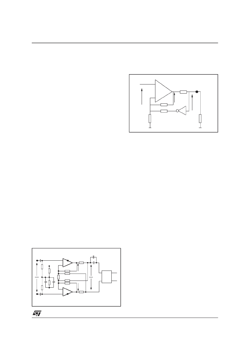
Let us consider the equivalent circuit for a single
ended configuration, figure4.
Figure 4 :
Single ended equivalent circuit
Let us consider the unloaded system. Assuming
the currents through R1, R2 and R3
as respectively:
1
As Vo
°
equals Vo without load, the gain in this
case becomes :
The gain, for the loaded system will be (1):
As shown in figure5, this system is an ideal gener-
ator with a synthesized impedance as the internal
impedance of the system. From this, the output
voltage becomes:
with Ro the synthesized impedance and Iout the
output current. On the other hand Vo can be ex-
pressed as:
2
1
2
R
3
R1
R4
R2
_
+
_
+
Vi
Vi
Vo
Vo
3
2
6
5
1
7
4
GND
8+12V
25
100
1:2
Hybrid
&
Transformer
GND
+12V
47k
47k
10
μ
100n
100n
100n
1k
1k
12.5
12.5
10n
1
μ
R3
R5
Vo
°
Vo
°
1/2
R1
R2
R3
+
_
Vi
Vo
Rs1
-1
Vo
°
1/2
RL
--------
--------–
andVi
°
(
)
Vo
+
R
3
)
,
G
Vi
)
------------------------------
1
----------------------------------
2
----------
2
3
------
+
+
1
2
R
3
------
–
=
=
GL
Vi
)
-----------------------------------
1
2
--
1
----------------------------------
1
2
----------
2
3
------
+
+
1
2
R
3
------
–
( )
,
=
=
Vo
ViG
(
)
RoIout
(
)
–
=
2
( )
,
Vo
Vi
1
----------------------------------------------
----------
2
------
+
+
1
------
–
---------------------
3
1
2
R
3
------
–
( )
,
–
=
相關(guān)PDF資料 |
PDF描述 |
|---|---|
| TS7920 | |
| TS805C06 | SCHOTTKY DIODE |
| TS805C04 | SCHOTTKY BARRIER DIODE |
| TS8388BCG | A/D CONVERTER |
| TSA2100G | TRIAC-FULL-WAVE-OUTPUT OPTOCOUPLER |
相關(guān)代理商/技術(shù)參數(shù) |
參數(shù)描述 |
|---|---|
| TS61N20CXRF | 制造商:TSC 制造商全稱:Taiwan Semiconductor Company, Ltd 功能描述:Voltage Detector |
| TS61N23CXRF | 制造商:TSC 制造商全稱:Taiwan Semiconductor Company, Ltd 功能描述:Voltage Detector |
| TS61N24CXRF | 制造商:TSC 制造商全稱:Taiwan Semiconductor Company, Ltd 功能描述:Voltage Detector |
| TS61N25CXRF | 制造商:TSC 制造商全稱:Taiwan Semiconductor Company, Ltd 功能描述:Voltage Detector |
| TS61N27CXRF | 制造商:TSC 制造商全稱:Taiwan Semiconductor Company, Ltd 功能描述:Voltage Detector |
發(fā)布緊急采購(gòu),3分鐘左右您將得到回復(fù)。