- 您現(xiàn)在的位置:買(mǎi)賣(mài)IC網(wǎng) > PDF目錄382685 > TR1003 Telecommunication IC PDF資料下載
參數(shù)資料
| 型號(hào): | TR1003 |
| 英文描述: | Telecommunication IC |
| 中文描述: | 通信集成電路 |
| 文件頁(yè)數(shù): | 9/12頁(yè) |
| 文件大小: | 111K |
| 代理商: | TR1003 |
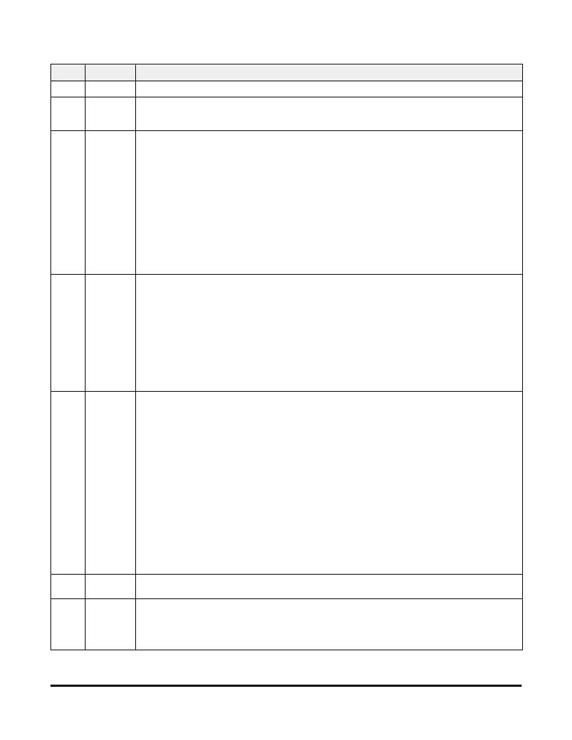
Pin
Name
Description
1
GND1
GND1 is the RF ground pin. GND2 and GND3 should be connected to GND1 by short, low-inductance traces.
2
VCC1
VCC1 is the positive supply voltage pin for the transmitter output amplifier and the receiver base-band circuitry.
VCC1 is usually connected to the positive supply through a ferrite RF decoupling bead, which is bypassed by an
RF capacitor on the
supply side
. See the
ASH Transceiver Designer’s Guide
for additional information.
3
AGCCAP
This pin controls the AGC reset operation. A capacitor between this pin and ground sets the minimum time the
AGC will hold-in once it is engaged. The hold-in time is set to avoid AGC chattering. For a given hold-in time t
AGH
,
the capacitor value C
AGC
is:
C
AGC
= 19.1* t
AGH
, where t
AGH
is in μs and C
AGC
is in pF
A ±10% ceramic capacitor should be used at this pin. The value of C
AGC
given above provides a hold-in time be-
tween t
AGH
and 2.65* t
AGH
, depending on operating voltage, temperature, etc. The hold-in time is chosen to allow
the AGC to ride through the longest run of zero bits that can occur in a received data stream. The AGC hold-in
time can be greater than the peak detector decay time, as discussed below. However, the AGC hold-in time
should not be set too long, or the receiver will be slow in returning to full sensitivity once the AGC is engaged by
noise or interference. The use of AGC is optional when using OOK modulation with data pulses of at least 30 μs.
AGC operation can be defeated by connecting this pin to Vcc. Active or latched AGC operation is required for
ASK modulation and/or for data pulses of less than 30 μs. The AGC can be latched on once engaged by connect-
ing a 150 K resistor between this pin and ground, instead of a capacitor. AGC operation depends on a functioning
peak detector, as discussed below. The AGC capacitor is discharged in the receiver power-down (sleep) mode
and in the transmit modes.
4
PKDET
This pin controls the peak detector operation. A capacitor between this pin and ground sets the peak detector at-
tack and decay times, which have a fixed 1:1000 ratio. For most applications, these time constants should be co-
ordinated with the base-band time constant. For a given base-band capacitor C
BBO
,
the capacitor value C
PKD
is:
C
PKD
= 0.33* C
BBO
, where C
BBO
and C
PKD
are in pF
A ±10% ceramic capacitor should be used at this pin. This time constant will vary between t
PKA
and 1.5* t
PKA
with
variations in supply voltage, temperature, etc. The capacitor is driven from a 200 ohm “attack” source, and decays
through a 200 K load. The peak detector is used to drive the “dB-below-peak” data slicer and the AGC release
function. The AGC hold-in time can be extended beyond the peak detector decay time with the AGC capacitor, as
discussed above. Where low data rates and OOK modulation are used, the “dB-below-peak” data slicer and the
AGC are optional. In this case, the PKDET pin and the THLD2 pin can be left unconnected, and the AGC pin can
be connected to Vcc to reduce the number of external components needed. The peak detector capacitor is dis-
charged in the receiver power-down (sleep) mode and in the transmit modes.
5
BBOUT
BBOUT is the receiver base-band output pin. This pin drives the CMPIN pin through a coupling capacitor C
BBO
for
internal data slicer operation. The time constant t
BBC
for this connection is:
t
BBC
= 0.064*C
BBO
, where t
BBC
is in μs and C
BBO
is in pF
A ±10% ceramic capacitor should be used between BBOUT and CMPIN. The time constant can vary between t
BBC
and 1.8*t
BBC
with variations in supply voltage, temperature, etc. The optimum time constant in a given circum-
stance will depend on the data rate, data run length, and other factors as discussed in the
ASH Transceiver De-
signer’s Guide
. A common criteria is to set the time constant for no more than a 20% voltage droop during SP
MAX
.
For this case:
C
BBO
= 70*SP
MAX
, where SP
MAX
is the maximum signal pulse width in μs and C
BBO
is in pF
The output from this pin can also be used to drive an external data recovery process (DSP, etc.). The nominal out-
put impedance of this pin is 1 K. When the receiver RF amplifiers are operating at a 50%-50% duty cycle, the
BBOUT signal changes about 10 mV/dB, with a peak-to-peak signal level of up to 685 mV. For lower duty cycles,
the mV/dB slope and peak-to-peak signal level are proportionately less. The signal at BBOUT is riding on a
1.1 Vdc value that varies somewhat with supply voltage and temperature, so it should be coupled through a ca-
pacitor to an external load. A load impedance of 50 K to 500 K in parallel with no more than 10 pF is recom-
mended. When an external data recovery process is used with AGC, BBOUT must be coupled to the external
data recovery process and CMPIN by separate series coupling capacitors. The AGC reset function is driven by
the signal applied to CMPIN. When the transceiver is in power-down (sleep) or in a transmit mode, the output im-
pedance of this pin becomes very high, preserving the charge on the coupling capacitor.
6
CMPIN
This pin is the input to the internal data slicers. It is driven from BBOUT through a coupling capacitor. The input
impedance of this pin is 70 K to 100 K.
7
RXDATA
RXDATA is the receiver data output pin. This pin will drive a 10 pF, 500 K parallel load. The peak current available
from this pin increases with the receiver low-pass filter cutoff frequency. In the power-down (sleep) or transmit
modes, this pin becomes high impedance. If required, a 1000 K pull-up or pull-down resistor can be used to estab-
lish a definite logic state when this pin is high impedance. If a pull-up resistor is used, the positive supply end
should be connected to a voltage no greater than Vcc + 200 mV.
9
Pin Descriptions
相關(guān)PDF資料 |
PDF描述 |
|---|---|
| TR112 | TIMER COUNTDOWN |
| TR118 | TIMER COUNTDOWN TWIN CHANNEL |
| TR117FA-0D30S | Optoelectronic |
| TR117FA-0D40S | Optoelectronic |
| TR133LA-0A10S | Telecomm/Datacomm |
相關(guān)代理商/技術(shù)參數(shù) |
參數(shù)描述 |
|---|---|
| TR1004 | 功能描述:射頻接收器 2G ASH Transceiver 914MHz 15.2 kbps RoHS:否 制造商:Skyworks Solutions, Inc. 類(lèi)型:GPS Receiver 封裝 / 箱體:QFN-24 工作頻率:4.092 MHz 工作電源電壓:3.3 V 封裝:Reel |
| TR1004PF31NB | 制造商:ITT Interconnect Solutions 功能描述:CABLE SOCKET TRIDENT 10/4 |
| TR1004PFS1NB | 制造商:ITT Interconnect Solutions 功能描述:JACK FREE 4WAY 制造商:ITT Interconnect Solutions 功能描述:JACK, FREE, 4WAY 制造商:ITT Interconnect Solutions 功能描述:JACK, FREE, 4WAY; Connector Type:Circular Industrial; Gender:Plug; Contact Gender:Socket; Connector Mounting:Cable; Connector Shell Size:10; Insert Arrangement:10-04; No. of Positions:4; SVHC:No SVHC (19-Dec-2012); Series:TRIDENT ;RoHS Compliant: Yes |
| TR1004PFS1NB | 制造商:ITT Interconnect Solutions 功能描述:JACK FREE 4 WAY |
| TR1004PMS1NB | 制造商:ITT Interconnect Solutions 功能描述:PLUG FREE 4WAY 制造商:ITT Interconnect Solutions 功能描述:PLUG, FREE, 4WAY 制造商:ITT Interconnect Solutions 功能描述:CIRCULAR CONN, PLUG, SZ 10-04, 4POS, CABLE; Connector Type:Circular Industrial; Connector Body Material:Nylon (Polyamide); Gender:Plug; Contact Gender:Socket; Connector Mounting:Cable; Connector Shell Size:10; Insert Arrangement:10-4;RoHS Compliant: Yes 制造商:ITT 功能描述:TRIDENT RINGLOCK UP TO 13 A CONTACT CURRENT RATING 制造商:ITT 功能描述:Conn Ringlock Circular PIN 4 POS Crimp ST Cable Mount 4 Terminal 1 Port |
發(fā)布緊急采購(gòu),3分鐘左右您將得到回復(fù)。