- 您現在的位置:買賣IC網 > PDF目錄98283 > TPS55383PWPRG4 (TEXAS INSTRUMENTS INC) 7 A DUAL SWITCHING CONTROLLER, 300 kHz SWITCHING FREQ-MAX, PDSO16 PDF資料下載
參數資料
| 型號: | TPS55383PWPRG4 |
| 廠商: | TEXAS INSTRUMENTS INC |
| 元件分類: | 穩(wěn)壓器 |
| 英文描述: | 7 A DUAL SWITCHING CONTROLLER, 300 kHz SWITCHING FREQ-MAX, PDSO16 |
| 封裝: | PLASTIC, HTSSOP-26 |
| 文件頁數: | 17/45頁 |
| 文件大小: | 1318K |
| 代理商: | TPS55383PWPRG4 |
第1頁第2頁第3頁第4頁第5頁第6頁第7頁第8頁第9頁第10頁第11頁第12頁第13頁第14頁第15頁第16頁當前第17頁第18頁第19頁第20頁第21頁第22頁第23頁第24頁第25頁第26頁第27頁第28頁第29頁第30頁第31頁第32頁第33頁第34頁第35頁第36頁第37頁第38頁第39頁第40頁第41頁第42頁第43頁第44頁第45頁
Dual Supply Operation
Cascading Supply Operation
1
2
3
4
16
15
14
13
PVDD2
BOOT2
SW2
BP
PVDD1
BOOT1
SW1
GND
TPS55383
5
6
7
12
11
10
SEQ
ILIM2
FB2
EN1
EN2
FB1
OUTPUT1
OUTPUT2
V
IN
UDG-08043
8
9
COMP2
COMP1
SLUS818 – SEPTEMBER 2008 ......................................................................................................................................................................................... www.ti.com
DESIGN HINT
The OCP threshold refers to the peak current in the internal switch. Be sure to add
one-half of the peak inductor ripple current to the dc load current in determining how
close the actual operating point is to the OCP threshold.
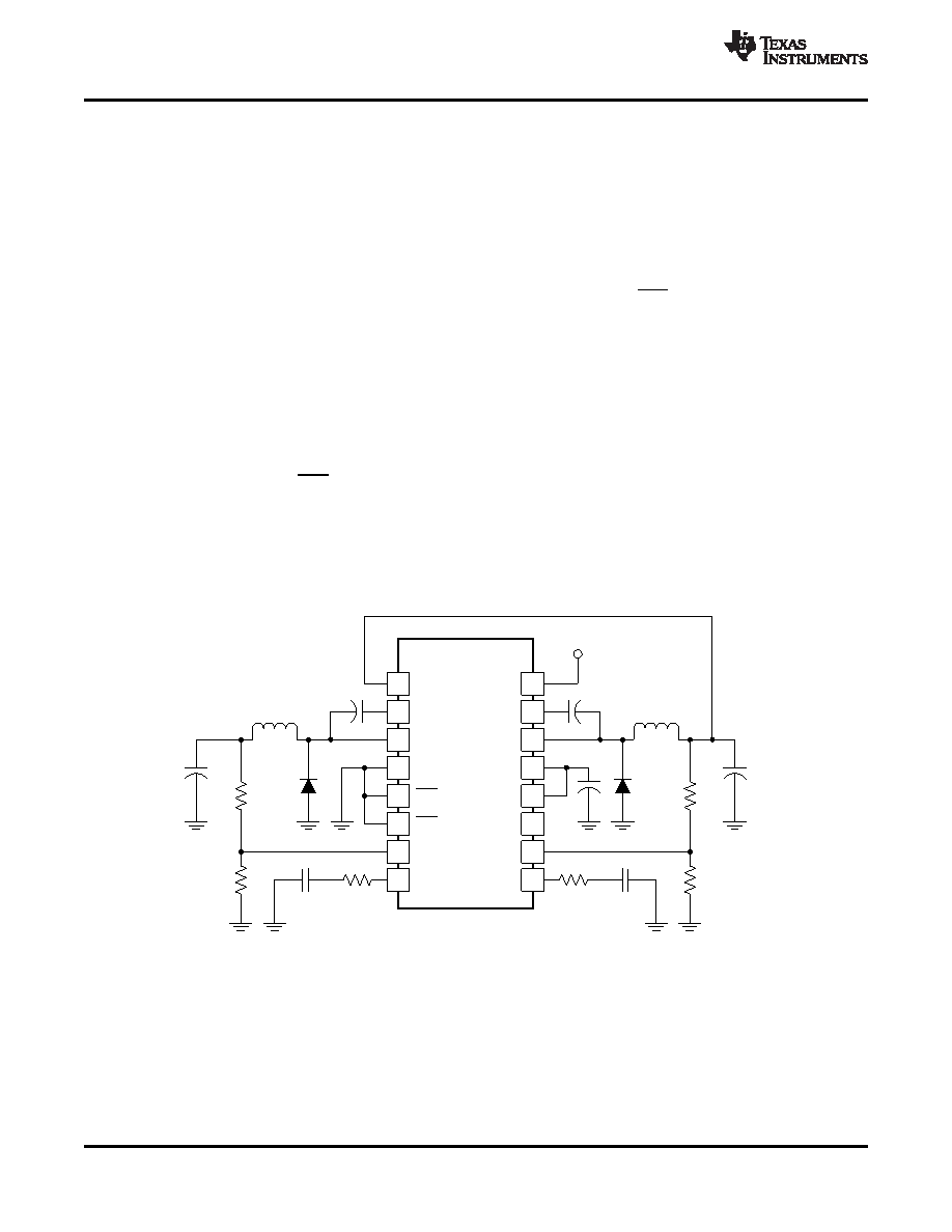
It is possible to operate a TPS5538x from two supply voltages. If this application is desired, then the sequencing
of the supplies must be such that PVDD2 is above the UVLO voltage before PVDD1 begins to rise. This level
requirement ensures that the internal regulator and the control circuitry are in operation before PVDD1 supplies
energy to the output. In addition, Output 1 must be held in the disabled state (EN1 high) until there is sufficient
voltage on PVDD1 to support Output 1 in regulation. (See the Operating Near Maximum Duty Cycle section.)
The preferred sequence of events is:
1. PVDD2 rises above the input UVLO voltage
2. PVDD1 rises with Output 1 disabled until PVDD1 rises above level to support Output 1 regulation.
With these two conditions satisfied, there is no restriction on PVDD2 to be greater than, or less than PVDD1.
DESIGN HINT
An R-C delay on EN1 may be used to delay the startup of Output 1 for a long enough
period of time to ensure that PVDD1 can support Output 1 load.
It is possible to source PVDD1 from Output 2 as depicted in Figure 27 and Figure 28. This configuration may be
preferred if the input voltage is high, relative to the voltage on Output 1.
Figure 27. Schematic Showing Cascading PVDD1 from Output 2
24
Copyright 2008, Texas Instruments Incorporated
相關PDF資料 |
PDF描述 |
|---|---|
| TPS5602IDBR | 3 A DUAL SWITCHING CONTROLLER, 500 kHz SWITCHING FREQ-MAX, PDSO30 |
| TPS5602IDBTRG4 | 3 A DUAL SWITCHING CONTROLLER, 202.4 kHz SWITCHING FREQ-MAX, PDSO30 |
| TPS5602IDBTR | 3 A DUAL SWITCHING CONTROLLER, 202.4 kHz SWITCHING FREQ-MAX, PDSO30 |
| TPS561000PWP | 1.4 A SWITCHING CONTROLLER, PDSO28 |
| TPS56100PWPR | 1.4 A SWITCHING CONTROLLER, 500 kHz SWITCHING FREQ-MAX, PDSO28 |
相關代理商/技術參數 |
參數描述 |
|---|---|
| TPS55386EVM-363 | 功能描述:電源管理IC開發(fā)工具 TPS55386EVM-363 Eval Mod RoHS:否 制造商:Maxim Integrated 產品:Evaluation Kits 類型:Battery Management 工具用于評估:MAX17710GB 輸入電壓: 輸出電壓:1.8 V |
| TPS55386PWP | 功能描述:直流/直流開關調節(jié)器 3A Dual Non-Synch Buck Converter RoHS:否 制造商:International Rectifier 最大輸入電壓:21 V 開關頻率:1.5 MHz 輸出電壓:0.5 V to 0.86 V 輸出電流:4 A 輸出端數量: 最大工作溫度: 安裝風格:SMD/SMT 封裝 / 箱體:PQFN 4 x 5 |
| TPS55386PWPG4 | 功能描述:直流/直流開關調節(jié)器 3A,Dual Non-Synch Buck Converter RoHS:否 制造商:International Rectifier 最大輸入電壓:21 V 開關頻率:1.5 MHz 輸出電壓:0.5 V to 0.86 V 輸出電流:4 A 輸出端數量: 最大工作溫度: 安裝風格:SMD/SMT 封裝 / 箱體:PQFN 4 x 5 |
| TPS55386PWPR | 功能描述:直流/直流開關調節(jié)器 3A Dual Non-Synch Buck Converter RoHS:否 制造商:International Rectifier 最大輸入電壓:21 V 開關頻率:1.5 MHz 輸出電壓:0.5 V to 0.86 V 輸出電流:4 A 輸出端數量: 最大工作溫度: 安裝風格:SMD/SMT 封裝 / 箱體:PQFN 4 x 5 |
| TPS55386PWPRG4 | 功能描述:直流/直流開關調節(jié)器 3A,Dual Non-Synch Buck Converter RoHS:否 制造商:International Rectifier 最大輸入電壓:21 V 開關頻率:1.5 MHz 輸出電壓:0.5 V to 0.86 V 輸出電流:4 A 輸出端數量: 最大工作溫度: 安裝風格:SMD/SMT 封裝 / 箱體:PQFN 4 x 5 |
發(fā)布緊急采購,3分鐘左右您將得到回復。