- 您現(xiàn)在的位置:買賣IC網(wǎng) > PDF目錄98280 > TPS24710DGS (TEXAS INSTRUMENTS INC) POWER SUPPLY SUPPORT CKT, PDSO10 PDF資料下載
參數(shù)資料
| 型號(hào): | TPS24710DGS |
| 廠商: | TEXAS INSTRUMENTS INC |
| 元件分類: | 電源管理 |
| 英文描述: | POWER SUPPLY SUPPORT CKT, PDSO10 |
| 封裝: | GREEN, PLASTIC, MSOP-10 |
| 文件頁(yè)數(shù): | 32/34頁(yè) |
| 文件大?。?/td> | 2148K |
| 代理商: | TPS24710DGS |
第1頁(yè)第2頁(yè)第3頁(yè)第4頁(yè)第5頁(yè)第6頁(yè)第7頁(yè)第8頁(yè)第9頁(yè)第10頁(yè)第11頁(yè)第12頁(yè)第13頁(yè)第14頁(yè)第15頁(yè)第16頁(yè)第17頁(yè)第18頁(yè)第19頁(yè)第20頁(yè)第21頁(yè)第22頁(yè)第23頁(yè)第24頁(yè)第25頁(yè)第26頁(yè)第27頁(yè)第28頁(yè)第29頁(yè)第30頁(yè)第31頁(yè)當(dāng)前第32頁(yè)第33頁(yè)第34頁(yè)
SLVSAL2C
– JANUARY 2011 – REVISED MAY 2011
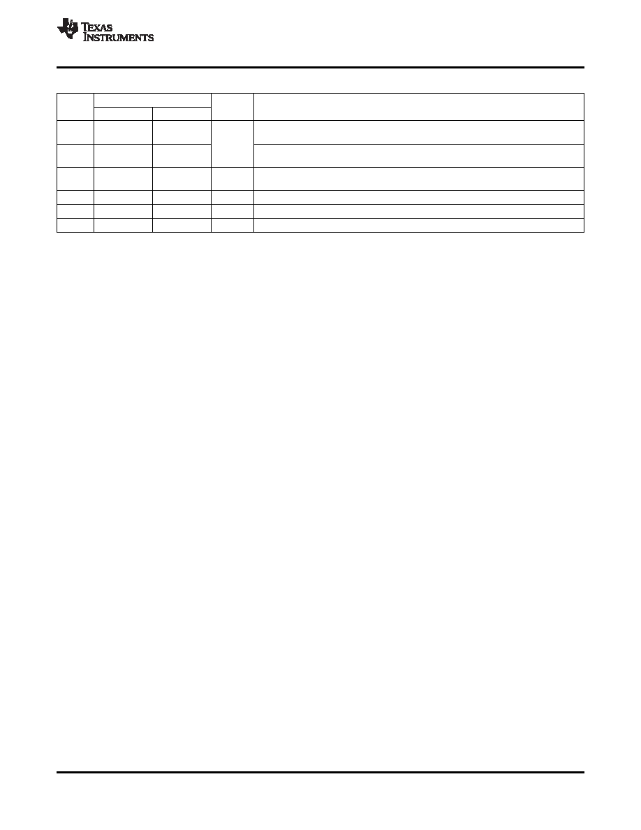
PIN FUNCTIONS (continued)
PINS
NAME
I/O
DESCRIPTION
TPS24710/11 TPS24712/13
Active-high, open-drain power good indicator. Status is determined by the voltage
PG
-
1
across the MOSFET.
O
Active-low, open-drain power good indicator. Status is determined by the voltage
PGb
1
-
across the MOSFET.
Power-limiting programming pin. A resistor from this pin to GND sets the maximum
PROG
3
I
power dissipation for the FET.
SENSE
8
I
Current sensing input for resistor shunt from VCC to SENSE.
TIMER
4
I/O
A capacitor connected from this pin to GND provides a fault timing function.
VCC
9
I
Input-voltage sense and power supply
DETAILED PIN DESCRIPTIONS
The following description relies on the typical application diagram on the front page of this data sheet, as well as
the functional block diagram in Figure 4.
EN: Applying a voltage of 1.35 V or more to this pin enables the gate driver. The addition of an external resistor
divider allows the EN pin to serve as an undervoltage monitor. Cycling EN low and then back high resets the
TPS24710/11/12/13 that has latched off due to a fault condition. This pin should not be left floating.
FLT: FLT is assigned for TPS24712/13. This active-high open-drain output assumes high-impedance when
TPS24712/13 has remained in current limit long enough for the fault timer to expire. The behavior of the FLT pin
depends on the version of the IC. The TPS24712 operates in latch mode and the TPS24713 operates in retry
mode. In latch mode, a fault timeout disables the external MOSFET and holds FLT in open drain condition. The
latched mode of operation is reset by cycling EN or VCC. In retry mode, a fault timeout first disables the external
MOSFET, next waits sixteen cycles of TIMER charging and discharging, and finally attempts a restart. This
process repeats as long as the fault persists. In retry mode, the FLT pin goes open-drain whenever the external
MOSFET is disabled by the fault timer. In a sustained fault, the FLT waveform becomes a train of pulses. The
FLT pin does not assert if the external MOSFET is disabled by EN, overtemperature shutdown, or UVLO. This
pin can be left floating when not used.
FLTb: FLTb is assigned for TPS24710/11. This active-low open-drain output pulls low when TPS24710/11/12/13
has remained in current limit long enough for the fault timer to expire. The behavior of the FLTb pin depends on
the version of the IC. The TPS24710 operates in latch mode and the TPS24711 operates in retry mode. In latch
mode, a fault timeout disables the external MOSFET and holds FLTb low. The latched mode of operation is reset
by cycling EN or VCC. In retry mode, a fault timeout first disables the external MOSFET, next waits sixteen
cycles of TIMER charging and discharging, and finally attempts a restart. This process repeats as long as the
fault persists. In retry mode, the FLTb pin is pulled low whenever the external MOSFET is disabled by the fault
timer. In a sustained fault, the FLTb waveform becomes a train of pulses. The FLTb pin does not assert if the
external MOSFET is disabled by EN, overtemperature shutdown, or UVLO. This pin can be left floating when not
used.
GATE: This pin provides gate drive to the external MOSFET. A charge pump sources 30
A to enhance the
external MOSFET. A 13.9-V clamp between GATE and VCC limits the gate-to-source voltage, because VVCC is
very close to VOUT in normal operation. During start-up, a transconductance amplifier regulates the gate voltage
of M1 to provide inrush current limiting. The TIMER pin charges timer capacitor CT during the inrush. Inrush
current limiting continues until the V(GATE – VCC) exceeds the Timer Activation Voltage (6 V for VVCC = 12 V). Then
the TPS24710/11/12/13 enters into circuit-breaker mode. The Timer Activation Voltage is defined as a threshold
voltage. When V(GATE-VCC) exceeds this threshold voltage, the inrush operation is finished and the TIMER stops
sourcing current and begins sinking current. In the circuit-breaker mode, the current flowing in RSENSE is
compared with the current-limit threshold derived from the MOSFET power-limit scheme (see PROG). If the
current flowing in RSENSE exceeds the current limit threshold, then MOSFET M1 is turned off. The GATE pin is
disabled by the following three conditions:
1. GATE is pulled down by an 11-mA current source when
– The fault timer expires during an overload current fault (VSENSE > 25 mV)
– VEN is below its falling threshold
Copyright
2011, Texas Instruments Incorporated
7
相關(guān)PDF資料 |
PDF描述 |
|---|---|
| TPS24710 | POWER SUPPLY SUPPORT CKT, PDSO10 |
| TPS24711 | POWER SUPPLY SUPPORT CKT, PDSO10 |
| TPS24711DGSR | POWER SUPPLY SUPPORT CKT, PDSO10 |
| TPS2481PW | POWER SUPPLY SUPPORT CKT, PDSO20 |
| TPS2480PW | POWER SUPPLY SUPPORT CKT, PDSO20 |
相關(guān)代理商/技術(shù)參數(shù) |
參數(shù)描述 |
|---|---|
| TPS24710DGSR | 功能描述:熱插拔功率分布 2.5-18V Hi Eff Hot- Swap Controller RoHS:否 制造商:Texas Instruments 產(chǎn)品:Controllers & Switches 電流限制: 電源電壓-最大:7 V 電源電壓-最小:- 0.3 V 工作溫度范圍: 功率耗散: 安裝風(fēng)格:SMD/SMT 封裝 / 箱體:MSOP-8 封裝:Tube |
| TPS24710EVM-003 | 功能描述:電源管理IC開(kāi)發(fā)工具 TPS24710 Eval Mod RoHS:否 制造商:Maxim Integrated 產(chǎn)品:Evaluation Kits 類型:Battery Management 工具用于評(píng)估:MAX17710GB 輸入電壓: 輸出電壓:1.8 V |
| TPS24711DGS | 功能描述:熱插拔功率分布 2.5-18V Hi Eff Hot- Swap Controller RoHS:否 制造商:Texas Instruments 產(chǎn)品:Controllers & Switches 電流限制: 電源電壓-最大:7 V 電源電壓-最小:- 0.3 V 工作溫度范圍: 功率耗散: 安裝風(fēng)格:SMD/SMT 封裝 / 箱體:MSOP-8 封裝:Tube |
| TPS24711DGSR | 功能描述:熱插拔功率分布 2.5-18V Hi Eff Hot- Swap Controller RoHS:否 制造商:Texas Instruments 產(chǎn)品:Controllers & Switches 電流限制: 電源電壓-最大:7 V 電源電壓-最小:- 0.3 V 工作溫度范圍: 功率耗散: 安裝風(fēng)格:SMD/SMT 封裝 / 箱體:MSOP-8 封裝:Tube |
| TPS24711EVM-004 | 功能描述:電源管理IC開(kāi)發(fā)工具 TPS24711 Eval Mod RoHS:否 制造商:Maxim Integrated 產(chǎn)品:Evaluation Kits 類型:Battery Management 工具用于評(píng)估:MAX17710GB 輸入電壓: 輸出電壓:1.8 V |
發(fā)布緊急采購(gòu),3分鐘左右您將得到回復(fù)。