- 您現(xiàn)在的位置:買賣IC網(wǎng) > PDF目錄368672 > TMS320F240PQA 16-Bit Microcontroller PDF資料下載
參數(shù)資料
| 型號(hào): | TMS320F240PQA |
| 英文描述: | 16-Bit Microcontroller |
| 中文描述: | 16位微控制器 |
| 文件頁數(shù): | 33/105頁 |
| 文件大小: | 1481K |
| 代理商: | TMS320F240PQA |
第1頁第2頁第3頁第4頁第5頁第6頁第7頁第8頁第9頁第10頁第11頁第12頁第13頁第14頁第15頁第16頁第17頁第18頁第19頁第20頁第21頁第22頁第23頁第24頁第25頁第26頁第27頁第28頁第29頁第30頁第31頁第32頁當(dāng)前第33頁第34頁第35頁第36頁第37頁第38頁第39頁第40頁第41頁第42頁第43頁第44頁第45頁第46頁第47頁第48頁第49頁第50頁第51頁第52頁第53頁第54頁第55頁第56頁第57頁第58頁第59頁第60頁第61頁第62頁第63頁第64頁第65頁第66頁第67頁第68頁第69頁第70頁第71頁第72頁第73頁第74頁第75頁第76頁第77頁第78頁第79頁第80頁第81頁第82頁第83頁第84頁第85頁第86頁第87頁第88頁第89頁第90頁第91頁第92頁第93頁第94頁第95頁第96頁第97頁第98頁第99頁第100頁第101頁第102頁第103頁第104頁第105頁
TMS320C240, TMS320F240
DSP CONTROLLERS
SPRS042D – OCTOBER 1996 – REVISED NOVEMBER 1998
33
POST OFFICE BOX 1443
HOUSTON, TEXAS 77251–1443
’x240 DSP core CPU
The TMS320x240 devices use an advanced Harvard-type architecture that maximizes processing power by
maintaining two separate memory bus structures — program and data — for full-speed execution. This multiple
bus structure allows data and instructions to be read simultaneously. Instructions support data transfers
between program memory and data memory. This architecture permits coefficients that are stored in program
memory to be read in RAM, thereby eliminating the need for a separate coefficient that are ROM. This, coupled
with a four-deep pipeline, allows the ’x240 devices to execute most instructions in a single cycle.
status and control registers
Two status registers, ST0 and ST1, contain the status of various conditions and modes. These registers can
be stored into data memory and loaded from data memory, thereby allowing the status of the machine to be
saved and restored for subroutines.
The load status register (LST) instruction is used to write to ST0 and ST1. The store status register (SST)
instruction is used to read from ST0 and ST1 — except for the INTM bit, which is not affected by the LST
instruction. The individual bits of these registers can be set or cleared when using the SETC and CLRC
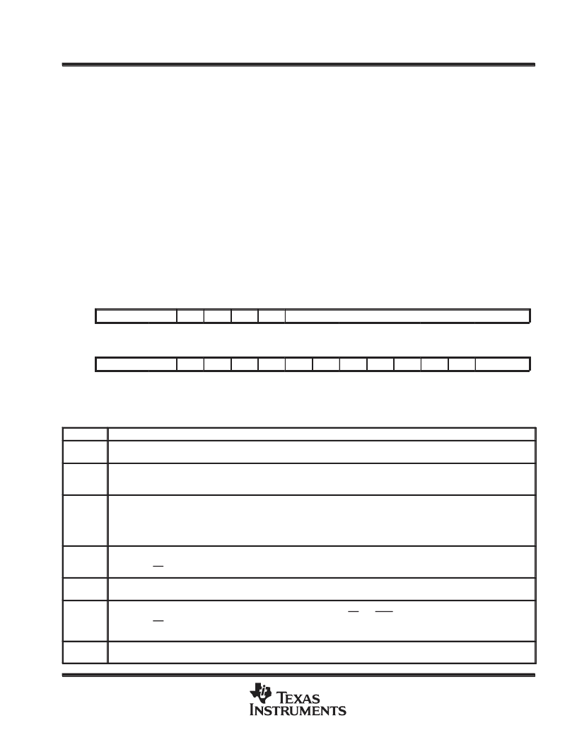
instructions. Figure 10 shows the organization of status registers ST0 and ST1, indicating all status bits
contained in each. Several bits in the status registers are reserved and are read as logic 1s. Table 11 lists status
register field definitions.
15
13
12
11
10
9
8
7
6
5
4
3
2
1
0
ST0
ARP
OV
OVM
1
INTM
DP
15
13
12
11
10
9
8
7
6
5
4
3
2
1
0
ST1
ARB
CNF
TC
SXM
C
1
1
1
1
XF
1
1
PM
Figure 10. Status and Control Register Organization
Table 11. Status Register Field Definitions
FIELD
FUNCTION
ARB
Auxiliary register pointer buffer. When the ARP is loaded into ST0, the old ARP value is copied to the ARB except during an LST
instruction. When the ARB is loaded by way of an LST #1 instruction, the same value is also copied to the ARP.
ARP
Auxiliary register (AR) pointer. ARP selects the AR to be used in indirect addressing. When the ARP is loaded, the old ARP value
is copied to the ARB register. ARP can be modified by memory-reference instructions when using indirect addressing, and by the
LARP, MAR, and LST instructions. The ARP is also loaded with the same value as ARB when an LST #1 instruction is executed.
C
Carry bit. C is set to 1 if the result of an addition generates a carry, or reset to 0 if the result of a subtraction generates a borrow.
Otherwise, C is reset after an addition or set after a subtraction, except if the instruction is ADD or SUB with a 16-bit shift. In these
cases, the ADD can only set and the SUB only reset the carry bit, but cannot affect it otherwise. The single bit shift and rotate
instructions also affect C, as well as the SETC, CLRC, and LST #1 instructions. Branch instructions have been provided to branch
on the status of C. C is set to 1 on a reset.
CNF
On-chip RAM configuration control bit. If CNF is set to 0, the reconfigurable data dual-access RAM blocks are mapped to data
space; otherwise, they are mapped to program space. The CNF can be modified by the SETC CNF, CLRC CNF, and LST #1
instructions. RS sets the CNF to 0.
DP
Data memory page pointer. The 9-bit DP register is concatenated with the seven LSBs of an instruction word to form a direct
memory address of 16 bits. DP can be modified by the LST and LDP instructions.
INTM
Interrupt mode bit. When INTM is set to 0, all unmasked interrupts are enabled. When set to 1, all maskable interrupts are disabled.
INTM is set and reset by the SETC INTM and CLRC INTM instructions. RS and IACK also set INTM. INTM has no effect on the
unmaskable RS and NMI interrupts. Note that INTM is unaffected by the LST instruction. This bit is set to 1 by reset. It is also set
to 1 when a maskable interrupt trap is taken.
OV
Overflow flag bit. As a latched overflow signal, OV is set to 1 when overflow occurs in the arithmetic logic unit (ALU). Once an
overflow occurs, the OV remains set until a reset, BCND/D on OV/NOV, or LST instructions clear OV.
相關(guān)PDF資料 |
PDF描述 |
|---|---|
| TMS320C240PQL | 16-Bit Microcontroller |
| TMS320C240PQQ | 16-Bit Microcontroller |
| TMS320F240PQL | 16-Bit Microcontroller |
| TMS320F240PQQ | 16-Bit Microcontroller |
| TMS320F240PQS | 16-Bit Microcontroller |
相關(guān)代理商/技術(shù)參數(shù) |
參數(shù)描述 |
|---|---|
| TMS320F240PQG4 | 功能描述:數(shù)字信號(hào)處理器和控制器 - DSP, DSC CMOS 320F240 BQFP TMS RoHS:否 制造商:Microchip Technology 核心:dsPIC 數(shù)據(jù)總線寬度:16 bit 程序存儲(chǔ)器大小:16 KB 數(shù)據(jù) RAM 大小:2 KB 最大時(shí)鐘頻率:40 MHz 可編程輸入/輸出端數(shù)量:35 定時(shí)器數(shù)量:3 設(shè)備每秒兆指令數(shù):50 MIPs 工作電源電壓:3.3 V 最大工作溫度:+ 85 C 封裝 / 箱體:TQFP-44 安裝風(fēng)格:SMD/SMT |
| TMS320F240PQS | 功能描述:數(shù)字信號(hào)處理器和控制器 - DSP, DSC 32B Dig Sig Cntrllr w/ Flash RoHS:否 制造商:Microchip Technology 核心:dsPIC 數(shù)據(jù)總線寬度:16 bit 程序存儲(chǔ)器大小:16 KB 數(shù)據(jù) RAM 大小:2 KB 最大時(shí)鐘頻率:40 MHz 可編程輸入/輸出端數(shù)量:35 定時(shí)器數(shù)量:3 設(shè)備每秒兆指令數(shù):50 MIPs 工作電源電壓:3.3 V 最大工作溫度:+ 85 C 封裝 / 箱體:TQFP-44 安裝風(fēng)格:SMD/SMT |
| TMS320F241FN | 功能描述:數(shù)字信號(hào)處理器和控制器 - DSP, DSC 16B 5V fixed point DSP w/ Flash RoHS:否 制造商:Microchip Technology 核心:dsPIC 數(shù)據(jù)總線寬度:16 bit 程序存儲(chǔ)器大小:16 KB 數(shù)據(jù) RAM 大小:2 KB 最大時(shí)鐘頻率:40 MHz 可編程輸入/輸出端數(shù)量:35 定時(shí)器數(shù)量:3 設(shè)備每秒兆指令數(shù):50 MIPs 工作電源電壓:3.3 V 最大工作溫度:+ 85 C 封裝 / 箱體:TQFP-44 安裝風(fēng)格:SMD/SMT |
| TMS320F241FN | 制造商:Texas Instruments 功能描述:IC C2000 DSP SMD 320F241 PLCC68 |
| TMS320F241FNA | 功能描述:數(shù)字信號(hào)處理器和控制器 - DSP, DSC 16B 5V fixed point DSP w/ Flash RoHS:否 制造商:Microchip Technology 核心:dsPIC 數(shù)據(jù)總線寬度:16 bit 程序存儲(chǔ)器大小:16 KB 數(shù)據(jù) RAM 大小:2 KB 最大時(shí)鐘頻率:40 MHz 可編程輸入/輸出端數(shù)量:35 定時(shí)器數(shù)量:3 設(shè)備每秒兆指令數(shù):50 MIPs 工作電源電壓:3.3 V 最大工作溫度:+ 85 C 封裝 / 箱體:TQFP-44 安裝風(fēng)格:SMD/SMT |
發(fā)布緊急采購,3分鐘左右您將得到回復(fù)。