- 您現(xiàn)在的位置:買賣IC網(wǎng) > PDF目錄368665 > TMS28F512A-15C3FME (Texas Instruments, Inc.) GT 26C 26#16 SKT PLUG PDF資料下載
參數(shù)資料
| 型號: | TMS28F512A-15C3FME |
| 廠商: | Texas Instruments, Inc. |
| 英文描述: | GT 26C 26#16 SKT PLUG |
| 中文描述: | 65536 8位快閃記憶體 |
| 文件頁數(shù): | 6/21頁 |
| 文件大小: | 311K |
| 代理商: | TMS28F512A-15C3FME |
TMS28F512A
65536 BY 8-BIT
FLASH MEMORY
SMJS514C – FEBRUARY 1994 – REVISED AUGUST 1997
6
POST OFFICE BOX 1443
HOUSTON, TEXAS 77251–1443
command register
The command register controls the program and erase functions of the TMS28F512A. The algorithm-selection
mode can be activated using the command register in addition to the previously described method. When V
PP
is high, the contents of the command register and the function being performed can be changed. The command
register is written to when E is low and W is pulsed low. The address is latched on the leading edge of the pulse,
while the data is latched on the trailing edge. Accidental programming or erasure is minimized because two
commands must be executed to invoke either operation.
power supply considerations
Each device should have a 0.1-
μ
F ceramic capacitor connected between V
CC
and V
SS
to suppress circuit noise.
Changes in current drain on V
PP
require it to have a bypass capacitor as well. Printed circuit traces for both
power supplies should be appropriate to handle the current demand.
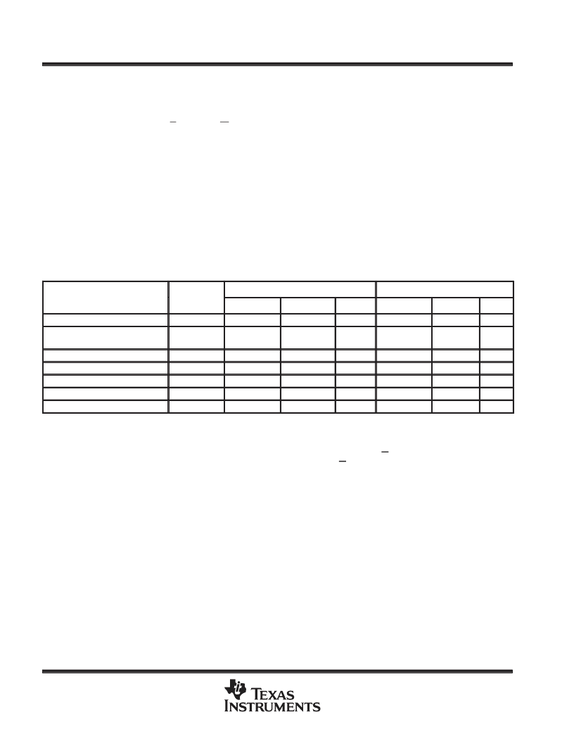
command definitions
See Table 3 for command definitions.
Table 3. Command Definitions
COMMAND
REQUIRED
BUS
CYCLES
FIRST BUS CYCLE
SECOND BUS CYCLE
OPERATION
ADDRESS
DATA
OPERATION
ADDRESS
DATA
Read
1
Write
X
00h
Read
RA
RD
Algorithm-Selection Mode
3
Write
X
90h
Read
0000
0001
89h
B8h
Set-Up-Erase/Erase
2
Write
X
20h
Write
X
20h
Erase Verify
2
Write
EA
A0h
Read
X
EVD
Set-Up-Program/Program
2
Write
X
40h
Write
PA
PD
Program Verify
2
Write
X
C0h
Read
X
PVD
Reset
Modes of operation are defined in Table 1
Legend:
EA
Address of memory location to be read during erase verify
EVD
Data read from location EA during erase verify
PA
Address of memory location to be programmed. Address is latched on the falling edge of W.
PD
Data to be programmed at location PA. Data is latched on the rising edge of W.
PVD
Data read from location PA during program verify
RA
Address of memory location to be read
RD
Data read from location RA during the read operation
2
Write
X
FFh
Write
X
FFh
read command
Memory contents can be accessed while V
PP
is high or low. When V
PP
is high, writing 00h into the command
register invokes the read operation. When the device is powered up, the default contents of the command
register are 00h and the read operation is enabled. The read operation remains enabled until a different valid
command is written to the command register.
algorithm-selection-mode command
The algorithm-selection mode is activated by writing 90h into the command register. The manufacturer
equivalent code (89h) is identified by the value read from address location 0000h, and the device equivalent
code (B8h) is identified by the value read from address location 0001h.
相關PDF資料 |
PDF描述 |
|---|---|
| TMS29F002RB-90BFML | x8 Flash EEPROM |
| TMS29F002RB-10BFME | x8 Flash EEPROM |
| TMS29F002RB-10CFME | x8 Flash EEPROM |
| TMS29F002RB-10CFML | x8 Flash EEPROM |
| TMS29F002RB-12BFME | x8 Flash EEPROM |
相關代理商/技術參數(shù) |
參數(shù)描述 |
|---|---|
| TMS29F040-12C5FML | 制造商:Texas Instruments 功能描述: |
| TMS29F04090C5FML | 制造商:TI 功能描述:* |
| TMS29F040-90C5FML | 制造商:Rochester Electronics LLC 功能描述:- Bulk |
| TMS29F04090C5FMLR | 制造商:TI 功能描述:* |
| TMS29F81606FML | 制造商:TI 功能描述:* |
發(fā)布緊急采購,3分鐘左右您將得到回復。