- 您現(xiàn)在的位置:買賣IC網(wǎng) > PDF目錄373637 > TH58NVG1S3AFT (Toshiba Corporation) TOSHIBA MOS DIGITAL INTEGRATED CIRCUIT SILICON GATE CMOS PDF資料下載
參數(shù)資料
| 型號(hào): | TH58NVG1S3AFT |
| 廠商: | Toshiba Corporation |
| 英文描述: | TOSHIBA MOS DIGITAL INTEGRATED CIRCUIT SILICON GATE CMOS |
| 中文描述: | 東芝馬鞍山數(shù)字集成電路硅柵CMOS |
| 文件頁數(shù): | 1/32頁 |
| 文件大小: | 368K |
| 代理商: | TH58NVG1S3AFT |
當(dāng)前第1頁第2頁第3頁第4頁第5頁第6頁第7頁第8頁第9頁第10頁第11頁第12頁第13頁第14頁第15頁第16頁第17頁第18頁第19頁第20頁第21頁第22頁第23頁第24頁第25頁第26頁第27頁第28頁第29頁第30頁第31頁第32頁
2003-05-19A
1/32
TH58NVG1S3AFT05
TENTATIVE
TOSHIBA MOS DIGITAL INTEGRATED CIRCUIT SILICON GATE CMOS
2GBIT (256M
u
8BITS) CMOS NAND E
2
PROM
DESCRIPTION
The TH58NVG1S3A is a single 3.3-V 2G-bit (2,214,592,512 bits) NAND Electrically Erasable and
Programmable Read-Only Memory (NAND E
2
PROM) organized as (2048+64) bytes x 64 pages x 2048 blocks.
The device has a 2112-byte static registers which allow program and read data to be transferred
between the register and the memory cell array in 2112-byte increments. The Erase operation is
implemented in a single block unit (128 Kbytes + 4Kbytes: 2112 bytes x 64 pages).
The TH58NVG1S3A is a serial-type memory device which utilizes the I/O pins for both address and data
input / output as well as for command inputs. The Erase and Program operations are automatically
executed making the device most suitable for applications such as solid-state file storage, voice
recording, image file memory for still cameras and other systems which require high-density non-
volatile memory data storage.
FEATURES
x
Organization
Memory cell allay 2112
u
64K
u
8
u
2
Register
Page size
Block size
Modes
Read
Reset
Auto Page Program
Auto Block Erase
Status Read
Mode control
Serial input
output
Command control
2112
u
8
2112bytes
(128K 4K) bytes
x
x
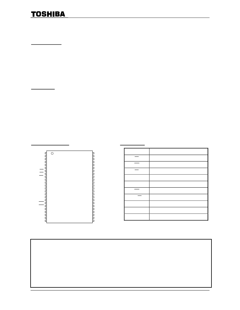
PIN ASSIGNMENT
(TOP VIEW)
PIN NAMES
I/O1 to I/O8
I/O port
CE
Chip enable
WE
Write enable
RE
Read enable
CLE
Command latch enable
ALE
Address latch enable
WP
Write protect
BY
/
RY
Ready / Busy
GND
Ground Input
V
CC
Power supply
V
SS
Ground
x
x
x
Powersupply V
CC
2.7 V to 3.6 V
Program/Erase Cycles 1E5 Cycles(With ECC)
Access time
Cell array to register
Serial Read Cycle
Operating current
Read (50 ns cycle)
Program (avg.)
Erase (avg.)
Standby
x
Package
TSOP I 48-P-1220-0.50
(Weight : 0.53 g typ.)
25
P
s
max
50 ns min
x
10 mA typ.
10 mA typ.
10 mA typ.
50
P
A max
x
TOSHIBA is continually working to improve the quality and reliability of its products. Nevertheless, semiconductor devices in general
can malfunction or fail due to their inherent electrical sensitivity and vulnerability to physical stress. It is the responsibility of the buyer,
when utilizing TOSHIBA products, to comply with the standards of safety in making a safe design for the entire system, and to avoid
situations in which a malfunction or failure of such TOSHIBA products could cause loss of human life, bodily injury or damage to
property.
In developing your designs, please ensure that TOSHIBA products are used within specified operating ranges as set forth in the most
recent TOSHIBA products specifications. Also, please keep in mind the precautions and conditions set forth in the “Handling Guide for
Semiconductor Devices,” or “TOSHIBA Semiconductor Reliability Handbook” etc..
x
The TOSHIBA products listed in this document are intended for usage in general electronics applications (computer, personal
equipment, office equipment, measuring equipment, industrial robotics, domestic appliances, etc.). These TOSHIBA products are
neither intended nor warranted for usage in equipment that requires extraordinarily high quality and/or reliability or a malfunction or
failure of which may cause loss of human life or bodily injury (“Unintended Usage”). Unintended Usage include atomic energy control
instruments, airplane or spaceship instruments, transportation instruments, traffic signal instruments, combustion control instruments,
medical instruments, all types of safety devices, etc.. Unintended Usage of TOSHIBA products listed in this document shall be made at
the customer’s own risk.
000707EBA1
1
2
3
4
5
6
7
8
9
10
11
12
13
14
15
16
17
18
19
20
21
22
23
24
NC
NC
NC
NC
I/O8
I/O7
I/O6
I/O5
NC
NC
NC
V
CC
V
SS
NC
NC
NC
I/O4
I/O3
I/O2
I/O1
NC
NC
NC
NC
NC
NC
NC
NC
NC
GND
BY
/
RY
NC
V
CC
V
SS
NC
NC
CLE
ALE
WE
WP
NC
NC
NC
NC
NC
48
47
46
45
44
43
42
41
40
39
38
37
36
35
34
33
32
31
30
29
28
27
26
25
RE
NC
相關(guān)PDF資料 |
PDF描述 |
|---|---|
| TH58NVG1S3AFT05 | TOSHIBA MOS DIGITAL INTEGRATED CIRCUIT SILICON GATE CMOS |
| TH7804A | 50 AMP LATCHING POWER RELAY |
| TH7804ACC | 50 AMP LATCHING POWER RELAY |
| TH7813A | 50 MHz 1024/2048 Linear CCDs |
| TH7813ACC | 50 MHz 1024/2048 Linear CCDs |
相關(guān)代理商/技術(shù)參數(shù) |
參數(shù)描述 |
|---|---|
| TH58NVG1S3AFT05 | 制造商:TOSHIBA 制造商全稱:Toshiba Semiconductor 功能描述:TOSHIBA MOS DIGITAL INTEGRATED CIRCUIT SILICON GATE CMOS |
| TH58NVG1S3AFT05DBJ | 制造商:Toshiba America Electronic Components 功能描述: |
| TH58NVG4S0ETA20 | 制造商:Toshiba America Electronic Components 功能描述:NAND FLASH - Rail/Tube |
| TH58NVG4S0ETAK0 | 制造商:Toshiba America Electronic Components 功能描述:NAND FLASH - Rail/Tube |
| TH58NVG4S0FBAID | 制造商:Toshiba America Electronic Components 功能描述:16GB SLC NAND BGA 32NM LB 10X11 (EEPROM) - Trays |
發(fā)布緊急采購,3分鐘左右您將得到回復(fù)。