- 您現(xiàn)在的位置:買賣IC網(wǎng) > PDF目錄385914 > TCM129C16 (Texas Instruments, Inc.) Single-Chip PCM Codecs And Filters(組合編碼譯碼器/濾波器) PDF資料下載
參數(shù)資料
| 型號: | TCM129C16 |
| 廠商: | Texas Instruments, Inc. |
| 元件分類: | Codec |
| 英文描述: | Single-Chip PCM Codecs And Filters(組合編碼譯碼器/濾波器) |
| 中文描述: | 單芯片的PCM編解碼器和過濾器(組合編碼譯碼器/濾波器) |
| 文件頁數(shù): | 3/25頁 |
| 文件大小: | 556K |
| 代理商: | TCM129C16 |
TCM29C13, TCM29C14, TCM29C16, TCM29C17,
TCM129C13, TCM129C14, TCM129C16, TCM129C17
COMBINED SINGLE-CHIP PCM CODEC AND FILTER
SCTS011G – APRIL 1986 – REVISED JULY 1996
3
POST OFFICE BOX 655303
DALLAS, TEXAS 75265
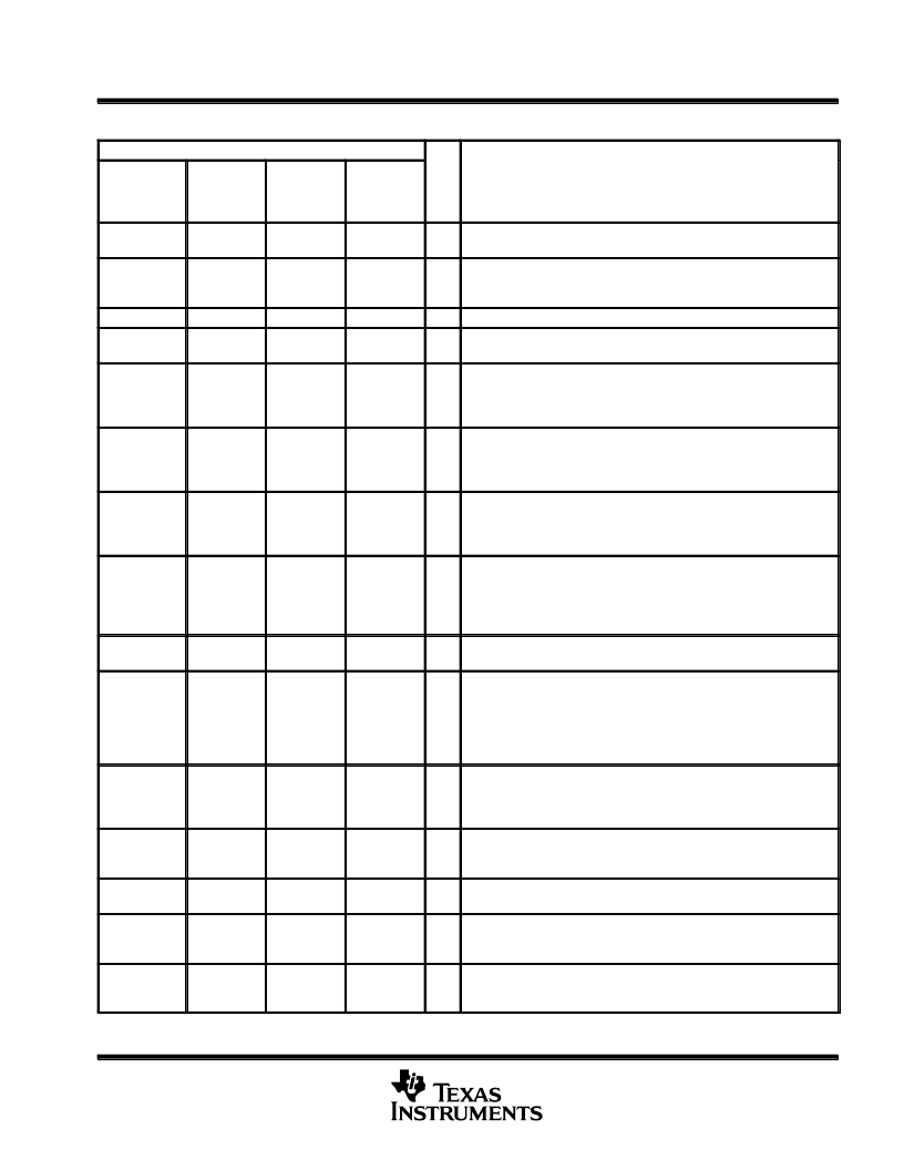
Terminal Functions
TERMINAL NO.
I/O
DESCRIPTION
NAME
TCM29C13
TCM129C13
TCM29C14
TCM129C14
TCM29C16
TCM29C17
TCM129C16
TCM129C17
13
ANLG GND
16
20
Analog ground return for all internal voice circuits. Not internally
connected to DGTL GND.
ANLG IN+
17
21
I
Noninverting analog input to uncommitted transmit operational amplifier.
Internally connected to ANLG GND on TCM129C16, TCM29C16,
TCM129C17, and TCM29C17.
ANLG IN–
18
22
14
I
Inverting analog input to uncommitted transmit operational amplifier.
ANLG LOOP
7
I
Provides loopback test capability. When this input is high, PWRO+ is
internally connected to ANLG IN.
CLKR
11
13
9
I
Receive master clock and data clock for the fixed-data-rate mode.
Receive master clock only for variable-data-rate mode. CLKR and CLKX
are internally connected together for TCM129C13, TCM129C16,
TCM129C17, TCM29C13, TCM29C16, and TCM29C17.
CLKSEL
6
6
I
Clock-frequency selection. Input must be connected to VBB, VCC, or
ground to reflect the master-clock frequency. When tied to VBB, CLK is
2.048 MHz. When tied to GND, CLK is 1.544 MHz. When tied to VCC,
CLK is 1.536 MHz.
CLKX
11
14
9
I
Transmit master clock and data clock for the fixed-data-rate mode.
Transmit master clock only for variable-date-rate mode. CLKR and
CLKX are internally connected for the TCM129C13, TCM129C16,
TCM129C17, TCM29C13, TCM29C16, and TCM29C17.
DCLKR
7
9
5
I
Fixed or variable-data-rate operation select. When connected to VBB,
the device operates in the fixed-data-rate mode. When DCLKR is not
connected to VBB, the device operates in the variable-data-rate mode,
and DCLKR becomes the receiver data clock. DCLKR then operates at
frequencies from 64 kHz to 2.048 MHz.
DGTL GND
10
12
8
Digital ground for all internal logic circuits. Not internally connected to
ANLG GND.
FSR/TSRE
9
11
7
I
Frame synchronization clock input/time-slot enable for receive channel.
In the fixed-data-rate mode, FSR distinguishes between signaling and
nonsignaling frames by a double- or single-length pulse, respectively. In
the variable-data-rate mode, this signal must remain high for the duration
of the time slot. The receive channel enters the standby state when FSR
is TTL low for 300 ms.
FSX/TSXE
12
15
10
I
Frame-synchronization clock input/time-slot enable for transmit
channel. Operates independently of, but in an analagous manner to,
FSR/TSRE. The transmit channel enters the standby state when FSX is
low for 300 ms.
GSR
4
4
I
Input to the gain-setting network on the output power amplifier.
Transmission level can be adjusted over a 12-dB range depending on the
voltage at GSR.
GSX
19
23
15
O
Output terminal of internal uncommitted operational amplifier. Internally,
this is the voice signal input to the transmit filter.
PCM IN
8
10
6
I
Receive PCM input. PCM data is clocked in on eight consecutive
negative transitions of the receive data clock, which is CLKR in
fixed-data-rate timing and DCLKR in variable-data-rate timing.
PCM OUT
13
16
11
O
Transmit PCM output. PCM data is clocked out on this output on eight
consecutive positive transitions of the transmit data clock, which is CLKX
in fixed-data-rate timing and DCLKX in variable-data-rate timing.
相關(guān)PDF資料 |
PDF描述 |
|---|---|
| TCM320AC36DW | VOICE-BAND AUDIO PROCESSORS VBAPE |
| TCM320AC36N | VOICE-BAND AUDIO PROCESSORS VBAPE |
| TCM320AC36PT | VOICE-BAND AUDIO PROCESSORS VBAPE |
| TCM320AC37DW | VOICE-BAND AUDIO PROCESSORS VBAPE |
| TCM320AC37N | VOICE-BAND AUDIO PROCESSORS VBAPE |
相關(guān)代理商/技術(shù)參數(shù) |
參數(shù)描述 |
|---|---|
| TCM129C16A | 制造商:TI 制造商全稱:Texas Instruments 功能描述:COMBINED SINGLE-CHIP PCM CODEC AND FILTER |
| TCM129C16ADW | 制造商:TI 制造商全稱:Texas Instruments 功能描述:COMBINED SINGLE-CHIP PCM CODEC AND FILTER |
| TCM129C16AN | 制造商:TI 制造商全稱:Texas Instruments 功能描述:COMBINED SINGLE-CHIP PCM CODEC AND FILTER |
| TCM129C16DW | 制造商:Rochester Electronics LLC 功能描述:- Bulk |
| TCM129C16N | 制造商:Rochester Electronics LLC 功能描述:- Bulk |
發(fā)布緊急采購,3分鐘左右您將得到回復。