- 您現(xiàn)在的位置:買賣IC網(wǎng) > PDF目錄373529 > T5753-6AQ (ATMEL CORP) UHF ASK/FSK TRANSMITTER PDF資料下載
參數(shù)資料
| 型號(hào): | T5753-6AQ |
| 廠商: | ATMEL CORP |
| 元件分類: | 通信及網(wǎng)絡(luò) |
| 英文描述: | UHF ASK/FSK TRANSMITTER |
| 中文描述: | SPECIALTY TELECOM CIRCUIT, PDSO8 |
| 封裝: | TSSOP-8 |
| 文件頁數(shù): | 5/13頁 |
| 文件大?。?/td> | 213K |
| 代理商: | T5753-6AQ |
5
T5753
4510F–RKE–07/04
Output Matching and Power
Setting
The output power is set by the load impedance of the antenna. The maximum output
power is achieved with a load impedance of Z
Load,opt
= (255 + j192)
. There must be a
low resistive path to V
S
to deliver the DC current.
The delivered current pulse of the power amplifier is 9 mA and the maximum output
power is delivered to a resistive load of 400
if the 1.0 pF output capacitance of the
power amplifier is compensated by the load impedance.
An optimum load impedance of:
Z
Load
= 400
|| j/(2
× π
1.0 pF) = (255 + j192)
thus results for the maximum output
power of 8 dBm.
The load impedance is defined as the impedance seen from the T5753’s ANT1, ANT2
into the matching network. Do not confuse this large signal load impedance with a small
signal input impedance delivered as input characteristic of RF amplifiers and measured
from the application into the IC instead of from the IC into the application for a power
amplifier.
Less output power is achieved by lowering the real parallel part of 400
where the
parallel imaginary part should be kept constant.
Output power measurement can be done with the circuit of Figure 5. Note that the com-
ponent values must be changed to compensate the individual board parasitics until the
T5753 has the right load impedance Z
Load,opt
= (255 + j192)
. Also the damping of the
cable used to measure the output power must be calibrated out.
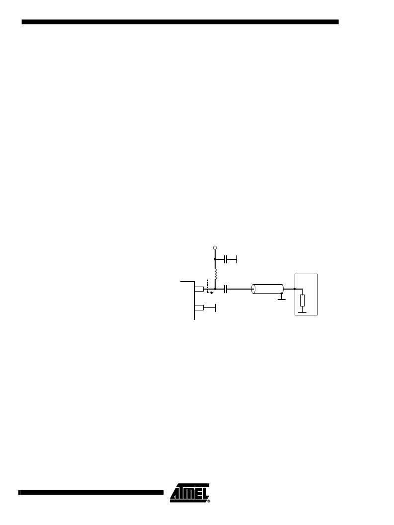
Figure 5.
Output Power Measurement
Application Circuit
For the blocking of the supply voltage a capacitor value of C
3
= 68 nF/X7R is recom-
mended (see Figure 6 on page 6 and Figure 7 on page 7). C
1
and C
2
are used to match
the loop antenna to the power amplifier where C
1
typically is 22 pF/NP0 and C
2
is
10.8 pF/NP0 (18 pF + 27 pF in series); for C
2
two capacitors in series should be used to
achieve a better tolerance value and to have the possibility to realize the Z
Load,opt
by
using standard valued capacitors.
C
1
forms together with the pins of T5753 and the PCB board wires a series resonance
loop that suppresses the 1
st
harmonic, hence the position of C
1
on the PCB is important.
Normally the best suppression is achieved when C
1
is placed as close as possible to the
pins ANT1 and ANT2.
The loop antenna should not exceed a width of 1.5 mm, otherwise the Q-factor of the
loop antenna is too high.
L
1
([50 nH to 100 nH) can be printed on PCB. C
4
should be selected that the XTO runs
on the load resonance frequency of the crystal. Normally, a value of 12 pF results for a
15 pF load-capacitance crystal.
~
~
ANT2
ANT1
R
in
50
Power
meter
C
1
= 1n
L
1
= 56n
C
2
= 3.3p
Z
Lopt
V
S
Z = 50
相關(guān)PDF資料 |
PDF描述 |
|---|---|
| T5754 | UHF ASK/FSK TRANSMITTER |
| T5754-6AQ | UHF ASK/FSK TRANSMITTER |
| T5760 | UHF ASK/FSK Receiver |
| T5760-TG | UHF ASK/FSK Receiver |
| T5761 | UHF ASK/FSK Receiver |
相關(guān)代理商/技術(shù)參數(shù) |
參數(shù)描述 |
|---|---|
| T5753-6AQJ | 功能描述:射頻發(fā)射器 ASK/FSK Transmitter 310 - 330 MHz RoHS:否 制造商:Micrel 類型:ASK Transmitter 封裝 / 箱體:SOT-23-6 工作頻率:300 MHz to 450 MHz 封裝:Reel |
| T5753-6AQJ 71 | 制造商:Atmel Corporation 功能描述:UHF ASK/FSK TRANSMITTER 315 MH |
| T5753-6AQJ 71 | 制造商:Atmel Corporation 功能描述:UHF ASK/FSK TRANSMITTER 315 MHZ - Tape and Reel |
| T5753-6AQJ-66 | 功能描述:射頻發(fā)射器 UHF ASK/FSK Trnsmttr 315 MHz RoHS:否 制造商:Micrel 類型:ASK Transmitter 封裝 / 箱體:SOT-23-6 工作頻率:300 MHz to 450 MHz 封裝:Reel |
| T5753-6AQJ71 | 功能描述:射頻發(fā)射器 UHF ASK/FSK Transmitter 315MHz RoHS:否 制造商:Micrel 類型:ASK Transmitter 封裝 / 箱體:SOT-23-6 工作頻率:300 MHz to 450 MHz 封裝:Reel |
發(fā)布緊急采購,3分鐘左右您將得到回復(fù)。