- 您現(xiàn)在的位置:買(mǎi)賣(mài)IC網(wǎng) > PDF目錄98148 > STK17TA8-R35 REAL TIME CLOCK, PDSO48 PDF資料下載
參數(shù)資料
| 型號(hào): | STK17TA8-R35 |
| 元件分類(lèi): | 時(shí)鐘/數(shù)據(jù)恢復(fù)及定時(shí)提取 |
| 英文描述: | REAL TIME CLOCK, PDSO48 |
| 封裝: | 0.300 INCH, 0.025 INCH PITCH, PLASTIC, SSOP-48 |
| 文件頁(yè)數(shù): | 6/25頁(yè) |
| 文件大?。?/td> | 285K |
| 代理商: | STK17TA8-R35 |
第1頁(yè)第2頁(yè)第3頁(yè)第4頁(yè)第5頁(yè)當(dāng)前第6頁(yè)第7頁(yè)第8頁(yè)第9頁(yè)第10頁(yè)第11頁(yè)第12頁(yè)第13頁(yè)第14頁(yè)第15頁(yè)第16頁(yè)第17頁(yè)第18頁(yè)第19頁(yè)第20頁(yè)第21頁(yè)第22頁(yè)第23頁(yè)第24頁(yè)第25頁(yè)

STK17TA8
April 2005
Document Control #ML0025 rev 1.1
14
Internally, RECALL is a two-step procedure. First,
the SRAM data is cleared, and second, the
nonvolatile information is transferred into the SRAM
cells. After the tRECALL cycle time the SRAM will once
again be ready for READ and WRITE operations.
The RECALL operation in no way alters the data in
the nonvolatile elements.
PREVENTING AUTOSTORE
TM
The AutoStore function can be disabled by initiat-
ing an AutoStore Disable sequence. A sequence of
read operations is performed in a manner similar to
the software STORE initiation. To initiate the
AutoStore Disable
sequence, the following sequence
of E controlled read operations must be performed:
1. Read address
0x4E38
Valid READ
2. Read address
0xB1C7
Valid READ
3. Read address
0x83E0
Valid READ
4. Read address
0x7C1F
Valid READ
5. Read address
0x703F
Valid READ
6. Read address
0x8B45
AutoStore Disable
The AutoStore can be re-enabled by initiating an
AutoStore Enable
sequence. A sequence of read
operations is performed in a manner similar to the
software RECALL initiation. To initiate the AutoStore
Enable
sequence, the following sequence of E
controlled read operations must be performed:
1. Read address
0x4E38
Valid READ
2. Read address
0xB1C7
Valid READ
3. Read address
0x83E0
Valid READ
4. Read address
0x7C1F
Valid READ
5. Read address
0x703F
Valid READ
6.
Read address
0x4B46
AutoStore Enable
If the AutoStore function is disabled or re-enabled
a manual STORE operation (Hardware or Software)
needs to be issued to save the AutoStore state
through subsequent power down cycles. The part
comes from the factory with AutoStore enabled.
DATA PROTECTION
The STK17TA8 protects data from corruption during
low-voltage conditions by inhibiting all externally
initiated STORE and WRITE operations. The low-
voltage condition is detected when VCC < VSWITCH .
If the STK17TA8 is in a WRITE mode (both E and
W
low ) at power-up, after a RECALL, or after a
STORE, the WRITE will be inhibited until a negative
transition on E or W
is detected. This protects
against inadvertent writes during power up or brown
out conditions.
NOISE CONSIDERATIONS
The STK17TA8 is a high-speed memory and so must
have
a
high-frequency
bypass
capacitor
of
approximately 0.1
F connected between VCC and VSS,
using leads and traces that are as short as possible.
As with all high-speed CMOS ICs, careful routing of
power, ground and signals will reduce circuit noise.
LOW AVERAGE ACTIVE POWER
CMOS technology provides the STK17TA8 this the
benefit of drawing significantly less current when it is
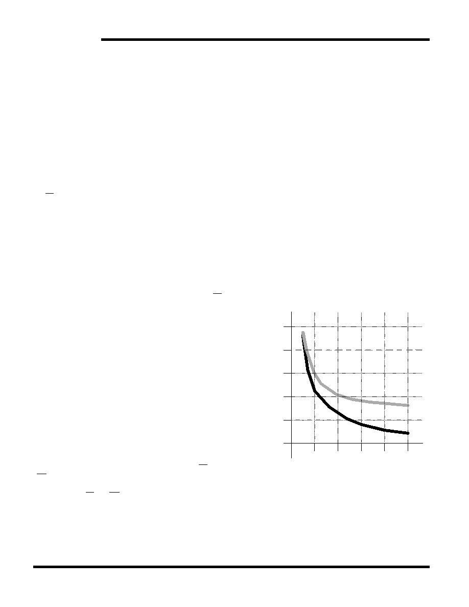
cycled at times longer than 50ns. Figure 6 shows the
relationship between ICC and READ/WRITE cycle
time. Worst-case current consumption is shown for
commercial temperature range, VCC = 3.6V, and chip
enable at maximum frequency. Only standby current
is drawn when the chip is disabled. The overall
average current drawn by the STK17TA8 depends on
the following items:
1. The duty cycle of chip enable.
2. The overall cycle rate for accesses.
3. The ratio of READs to WRITEs.
4. The operating temperature.
5. The VCC level.
6. I/O loading.
Ave
rag
e
A
cti
ve
Cu
rre
nt
(mA)
100 150 200 300
0
10
20
30
40
50
Writes
Reads
Cycle Time (ns)
50
Figure 6 Current vs. Cycle time
相關(guān)PDF資料 |
PDF描述 |
|---|---|
| STK17TA8-W25 | REAL TIME CLOCK, PDIP40 |
| STK17TA8-R45 | REAL TIME CLOCK, PDSO48 |
| STK17TA8-R25 | REAL TIME CLOCK, PDSO48 |
| STK17TA8RF25I | REAL TIME CLOCK, PDSO48 |
| STLED316SMTR | 4 X 17 SEGMENTS SEGMENT LED DRVR AND DSPL CTLR, PDSO24 |
相關(guān)代理商/技術(shù)參數(shù) |
參數(shù)描述 |
|---|---|
| STK17TA8-RF25 | 功能描述:NVRAM 128Kbx8+RTC 2.7-3.6V RoHS:否 制造商:Maxim Integrated 數(shù)據(jù)總線寬度:8 bit 存儲(chǔ)容量:1024 Kbit 組織:128 K x 8 接口類(lèi)型:Parallel 訪問(wèn)時(shí)間:70 ns 電源電壓-最大:5.5 V 電源電壓-最小:4.5 V 工作電流:85 mA 最大工作溫度:+ 70 C 最小工作溫度:0 C 封裝 / 箱體:EDIP 封裝:Tube |
| STK17TA8-RF25I | 功能描述:NVRAM 128Kbx8+RTC 2.7-3.6V RoHS:否 制造商:Maxim Integrated 數(shù)據(jù)總線寬度:8 bit 存儲(chǔ)容量:1024 Kbit 組織:128 K x 8 接口類(lèi)型:Parallel 訪問(wèn)時(shí)間:70 ns 電源電壓-最大:5.5 V 電源電壓-最小:4.5 V 工作電流:85 mA 最大工作溫度:+ 70 C 最小工作溫度:0 C 封裝 / 箱體:EDIP 封裝:Tube |
| STK17TA8-RF25IL | 制造商:Cypress Semiconductor 功能描述: |
| STK17TA8-RF25ITR | 功能描述:NVRAM 128Kbx8+RTC 2.7-3.6V RoHS:否 制造商:Maxim Integrated 數(shù)據(jù)總線寬度:8 bit 存儲(chǔ)容量:1024 Kbit 組織:128 K x 8 接口類(lèi)型:Parallel 訪問(wèn)時(shí)間:70 ns 電源電壓-最大:5.5 V 電源電壓-最小:4.5 V 工作電流:85 mA 最大工作溫度:+ 70 C 最小工作溫度:0 C 封裝 / 箱體:EDIP 封裝:Tube |
| STK17TA8-RF25TR | 功能描述:NVRAM 128Kbx8+RTC 2.7-3.6V RoHS:否 制造商:Maxim Integrated 數(shù)據(jù)總線寬度:8 bit 存儲(chǔ)容量:1024 Kbit 組織:128 K x 8 接口類(lèi)型:Parallel 訪問(wèn)時(shí)間:70 ns 電源電壓-最大:5.5 V 電源電壓-最小:4.5 V 工作電流:85 mA 最大工作溫度:+ 70 C 最小工作溫度:0 C 封裝 / 箱體:EDIP 封裝:Tube |
發(fā)布緊急采購(gòu),3分鐘左右您將得到回復(fù)。