- 您現(xiàn)在的位置:買賣IC網(wǎng) > PDF目錄385861 > SSTVN16859 (NXP Semiconductors N.V.) 13-bit 1:2 SSTL_2 registered buffer for DDR PDF資料下載
參數(shù)資料
| 型號: | SSTVN16859 |
| 廠商: | NXP Semiconductors N.V. |
| 英文描述: | 13-bit 1:2 SSTL_2 registered buffer for DDR |
| 中文描述: | 13位1:2 SSTL_2登記緩沖區(qū)的DDR |
| 文件頁數(shù): | 7/11頁 |
| 文件大?。?/td> | 116K |
| 代理商: | SSTVN16859 |
Philips Semiconductors
Product data sheet
SSTVN16859
13-bit 1:2 SSTL_2 registered buffer for DDR
2004 Jul 15
7
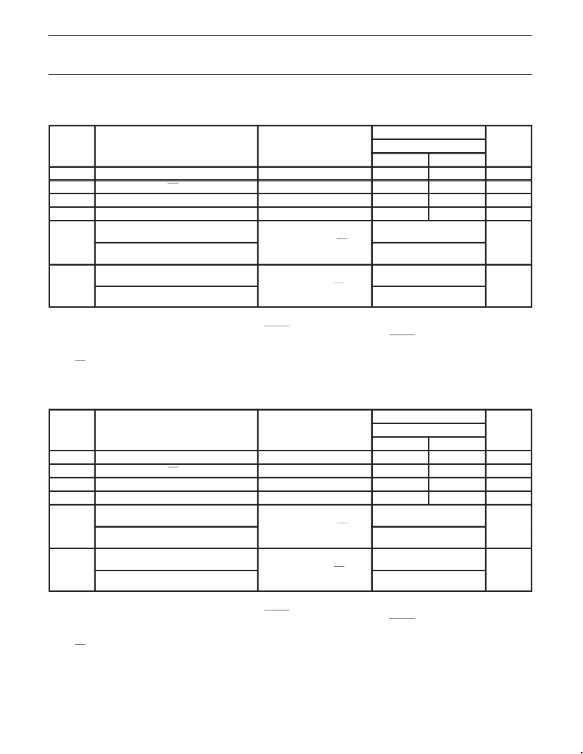
TIMING REQUIREMENTS—PC1600–PC2700
Over recommended operating conditions; T
amb
= 0
°
C to +70
°
C (unless otherwise noted) (see Figure 1)
LIMITS
SYMBOL
PARAMETER
TEST CONDITIONS
V
DD
= 2.5 V
±
0.2 V
MIN
UNIT
MAX
f
clock
t
w
t
act
t
inact
Clock frequency
—
200
MHz
Pulse duration, CK, CK HIGH or LOW
2.5
—
ns
Differential inputs active time
Notes 1, 2
—
22
ns
Differential inputs inactive time
Notes 1, 3
—
22
ns
t
su
Setup time, fast slew rate
(see Notes 4 and 6)
Data before CK
↑
, CK
↓
0.65
ns
Setup time, slow slew rate
(see Notes 5 and 6)
0.75
t
h
Hold time, fast slew rate
(see Notes 4 and 6)
Data after CK
↑
, CK
↓
0.75
ns
Hold time, slow slew rate
(see Notes 5 and 6)
0.9
NOTES:
1. This parameter is not necessarily production tested.
2. Data inputs must be below a minimum time of t
act
max, after RESET is taken HIGH.
3. Data and clock inputs must be held at valid levels (not floating) a minimum time of t
inact
max, after RESET is taken LOW.
4. For data signal input slew rate
≥
1 V/ns.
5. For data signal input slew rate
≥
0.5 V/ns and < 1 V/ns.
6. CK, CK signals input slew rates are
≥
1 V/ns.
TIMING REQUIREMENTS—PC3200
Over recommended operating conditions; T
amb
= 0
°
C to +70
°
C (unless otherwise noted) (see Figure 1)
LIMITS
SYMBOL
PARAMETER
TEST CONDITIONS
V
DD
= 2.6 V
±
0.1 V
MIN
UNIT
MAX
f
clock
t
w
t
act
t
inact
Clock frequency
—
210
MHz
Pulse duration, CK, CK HIGH or LOW
2.5
—
ns
Differential inputs active time
Notes 1, 2
—
22
ns
Differential inputs inactive time
Notes 1, 3
—
22
ns
t
su
Setup time, fast slew rate
(see Notes 4 and 6)
Data before CK
↑
, CK
↓
0.65
ns
Setup time, slow slew rate
(see Notes 5 and 6)
0.75
t
h
Hold time, fast slew rate
(see Notes 4 and 6)
Data after CK
↑
, CK
↓
0.65
ns
Hold time, slow slew rate
(see Notes 5 and 6)
0.8
NOTES:
1. This parameter is not necessarily production tested.
2. Data inputs must be below a minimum time of t
act
max, after RESET is taken HIGH.
3. Data and clock inputs must be held at valid levels (not floating) a minimum time of t
inact
max, after RESET is taken LOW.
4. For data signal input slew rate
≥
1 V/ns.
5. For data signal input slew rate
≥
0.5 V/ns and < 1 V/ns.
6. CK, CK signals input slew rates are
≥
1 V/ns.
相關PDF資料 |
PDF描述 |
|---|---|
| SSTVN16859BS | 13-bit 1:2 SSTL_2 registered buffer for DDR |
| ST-114 | Downconverter Evaluatiuon Board |
| ST083S | INVERTER GRADE THYRISTORS Stud Version |
| ST083S08PFN1 | INVERTER GRADE THYRISTORS |
| ST083S10PFK0 | INVERTER GRADE THYRISTORS |
相關代理商/技術參數(shù) |
參數(shù)描述 |
|---|---|
| SSTVN16859BS | 功能描述:寄存器 13BIT 1:2 SSTL2 REG BUF/DDR RoHS:否 制造商:NXP Semiconductors 邏輯類型:CMOS 邏輯系列:HC 電路數(shù)量:1 最大時鐘頻率:36 MHz 傳播延遲時間: 高電平輸出電流:- 7.8 mA 低電平輸出電流:7.8 mA 電源電壓-最大:6 V 最大工作溫度:+ 125 C 封裝 / 箱體:SOT-38 封裝:Tube |
| SSTVN16859BS,118 | 功能描述:寄存器 13BIT 1:2 SSTL2 REG RoHS:否 制造商:NXP Semiconductors 邏輯類型:CMOS 邏輯系列:HC 電路數(shù)量:1 最大時鐘頻率:36 MHz 傳播延遲時間: 高電平輸出電流:- 7.8 mA 低電平輸出電流:7.8 mA 電源電壓-最大:6 V 最大工作溫度:+ 125 C 封裝 / 箱體:SOT-38 封裝:Tube |
| SSTVN16859BS,151 | 功能描述:寄存器 13BIT 1:2 SSTL2 REG RoHS:否 制造商:NXP Semiconductors 邏輯類型:CMOS 邏輯系列:HC 電路數(shù)量:1 最大時鐘頻率:36 MHz 傳播延遲時間: 高電平輸出電流:- 7.8 mA 低電平輸出電流:7.8 mA 電源電壓-最大:6 V 最大工作溫度:+ 125 C 封裝 / 箱體:SOT-38 封裝:Tube |
| SSTVN16859BS,157 | 功能描述:寄存器 13BIT 1:2 SSTL2 REG RoHS:否 制造商:NXP Semiconductors 邏輯類型:CMOS 邏輯系列:HC 電路數(shù)量:1 最大時鐘頻率:36 MHz 傳播延遲時間: 高電平輸出電流:- 7.8 mA 低電平輸出電流:7.8 mA 電源電壓-最大:6 V 最大工作溫度:+ 125 C 封裝 / 箱體:SOT-38 封裝:Tube |
| SSTVN16859BS-S | 功能描述:寄存器 13BIT 1:2 SSTL2 REG BUF/DDR RoHS:否 制造商:NXP Semiconductors 邏輯類型:CMOS 邏輯系列:HC 電路數(shù)量:1 最大時鐘頻率:36 MHz 傳播延遲時間: 高電平輸出電流:- 7.8 mA 低電平輸出電流:7.8 mA 電源電壓-最大:6 V 最大工作溫度:+ 125 C 封裝 / 箱體:SOT-38 封裝:Tube |
發(fā)布緊急采購,3分鐘左右您將得到回復。