- 您現(xiàn)在的位置:買賣IC網(wǎng) > PDF目錄225224 > SPT7861SCU (SIGNAL PROCESSING TECHNOLOGIES) 1-CH 10-BIT SUCCESSIVE APPROXIMATION ADC, PARALLEL ACCESS, UUC28 PDF資料下載
參數(shù)資料
| 型號: | SPT7861SCU |
| 廠商: | SIGNAL PROCESSING TECHNOLOGIES |
| 元件分類: | ADC |
| 英文描述: | 1-CH 10-BIT SUCCESSIVE APPROXIMATION ADC, PARALLEL ACCESS, UUC28 |
| 封裝: | DIE-28 |
| 文件頁數(shù): | 6/8頁 |
| 文件大小: | 91K |
| 代理商: | SPT7861SCU |
SPT
6
2/10/98
SPT7861
Figure 4 shows an example of expected voltage drops for a
specific case. VREF of 4.0 V is applied to VRHF and VRLF is
tied to AGND. A 90 mV drop is seen at VRHS (= 3.91 V) and
a 75 mV increase is seen at VRLS (= 0.075 V).
ANALOG INPUT
VIN is the analog input. The input voltage range is from VRLS to
VRHS(typically 4.0 V) and will scale proportionally with respect to
the voltage reference. (See the Voltage Reference section.)
The drive requirements for the analog inputs are very minimal
when compared to most other converters due to the SPT7861's
extremely low input capacitance of only 5 pF and very high
input resistance in excess of 50 k
.
The analog input should be protected through a series
resistor and diode clamping circuit as shown in figure 5.
CALIBRATION
The SPT7861 uses a user transparent, auto calibration
scheme to ensure 10-bit accuracy over time and tempera-
ture. Gain and offset errors are continually adjusted to 10-bit
accuracy during device operation.
Upon power-up, the SPT7861 begins its calibration algo-
rithm. In order to achieve the calibration accuracy required,
the offset and gain adjustment step size is a fraction of a 10-
bit LSB. Since the calibration algorithm is an oversampling
process, a minimum of 10,000 clock cycles are required.
This results in a minimum calibration time upon power-up of
250
sec (for a 40 MHz clock). Once calibrated, the SPT7861
remains calibrated over time and temperature.
Since the calibration cycles are initiated on the rising edge of
the clock, the clock must be continuously applied for the
SPT7861 to remain in calibration.
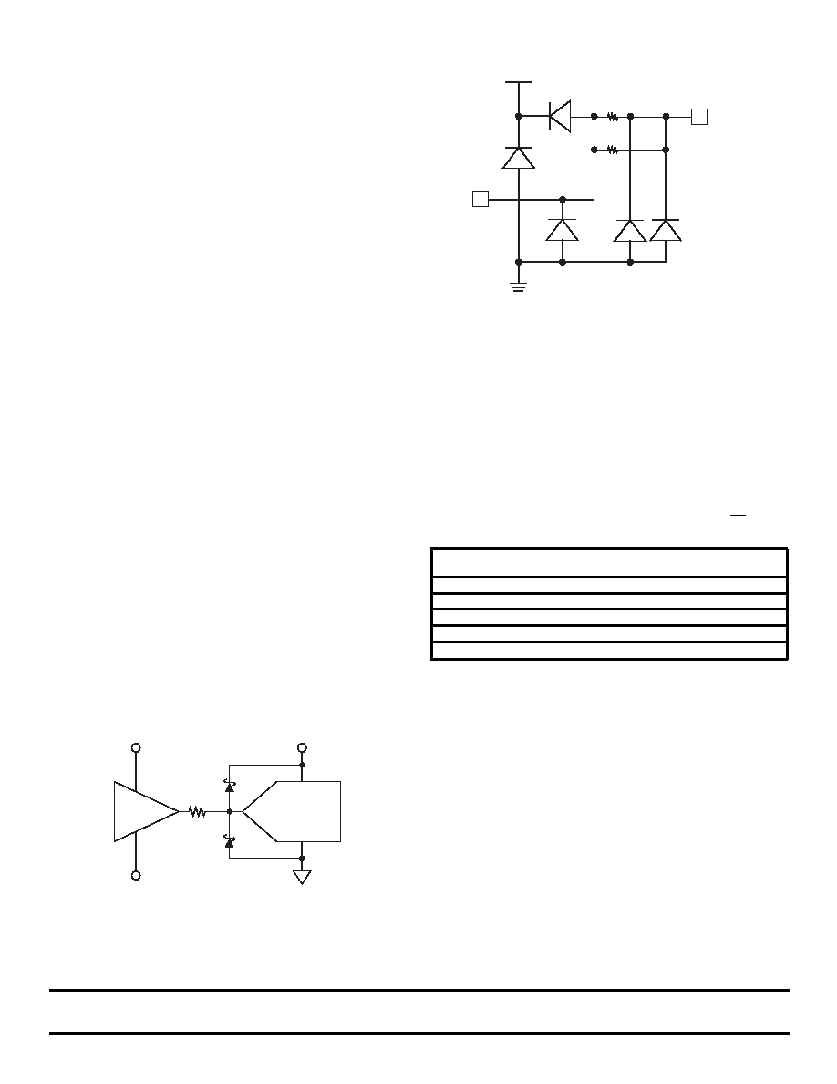
INPUT PROTECTION
All I/O pads are protected with an on-chip protection circuit
shown in figure 6. This circuit provides ESD robustness to
3.5 kV and prevents latch-up under severe discharge condi-
tions without degrading analog transition times.
Figure 6 - On-Chip Protection Circuit
VDD
Analog
Pad
120
120
CLOCK INPUT
The SPT7861 is driven from a single-ended TTL-input clock.
Because the pipelined architecture operates on the rising edge of
the clock input, the device can operate over a wide range of input
clock duty cycles without degrading the dynamic performance.
DIGITAL OUTPUTS
The digital outputs (D0-D10) are driven by a separate supply
(OVDD) ranging from +3 V to +5 V. This feature makes it
possible to drive the SPT7861's TTL/CMOS-compatible out-
puts with the user's logic system supply. The format of the
output data (D0-D9) is straight binary. (See table III.) The
outputs are latched on the rising edge of CLK. These outputs
can be switched into a tri-state mode by bringing EN high.
Table III - Output Data Information
ANALOG INPUT
OVERRANGE
OUTPUT CODE
D10
D9-D0
+F.S. + 1/2 LSB
1
11 1111
1111
+F.S. -1/2 LSB
O
11 1111
111
+1/2 F.S.
O
+1/2 LSB
O
OO OOOO OOO
0.0 V
O
OO OOOO OOOO
( indicates the flickering bit between logic 0 and 1).
OVERRANGE OUTPUT
The Overrange Output (D10) is an indication that the analog
input signal has exceeded the positive full scale input voltage
by 1 LSB. When this condition occurs, D10 will switch to
logic 1. All other data outputs (D0 to D9) will remain at logic 1
as long as D10 remains at logic 1. This feature makes it
possible to include the SPT7861 in higher resolution systems.
EVALUATION BOARD
The EB7861 evaluation board is available to aid designers in
demonstrating the full performance of the SPT7861. This
board includes a reference circuit, clock driver circuit, output
data latches and an on-board reconstruction of the digital
data. An application note describing the operation of this
board as well as information on the testing of the SPT7861 is
also available. Contact the factory for price and availability.
Figure 5 - Recommended Input Protection Circuit
47
D1
D2
ADC
Buffer
AVDD
+V
-V
D1 = D2 = Hewlett Packard HP5712 or equivalent
相關(guān)PDF資料 |
PDF描述 |
|---|---|
| SPT7862SIT | DUAL 1-CH 10-BIT SUCCESSIVE APPROXIMATION ADC, PARALLEL ACCESS, PQFP64 |
| SPT7862SIT | DUAL 1-CH 10-BIT SUCCESSIVE APPROXIMATION ADC, PARALLEL ACCESS, PQFP64 |
| SPT7866 | 1-CH 10-BIT PROPRIETARY METHOD ADC, PARALLEL ACCESS, PDSO28 |
| SPT7866 | 1-CH 10-BIT PROPRIETARY METHOD ADC, PARALLEL ACCESS, PDSO28 |
| SPT7868SIR | 1-CH 10-BIT PROPRIETARY METHOD ADC, PARALLEL ACCESS, PDSO28 |
相關(guān)代理商/技術(shù)參數(shù) |
參數(shù)描述 |
|---|---|
| SPT7862 | 制造商:CADEKA 制造商全稱:CADEKA 功能描述:10-BIT, 40 MSPS, DUAL-CHANNEL A/D CONVERTER |
| SPT7862SIT | 制造商:CADEKA 制造商全稱:CADEKA 功能描述:10-BIT, 40 MSPS, DUAL-CHANNEL A/D CONVERTER |
| SPT7863 | 制造商:FAIRCHILD 制造商全稱:Fairchild Semiconductor 功能描述:10-BIT, 40 MSPS, 160 mW A/D CONVERTER |
| SPT7863SCS | 功能描述:直流/直流開關(guān)轉(zhuǎn)換器 10BIT 40MSPS SaR aDC RoHS:否 制造商:STMicroelectronics 最大輸入電壓:4.5 V 開關(guān)頻率:1.5 MHz 輸出電壓:4.6 V 輸出電流:250 mA 輸出端數(shù)量:2 最大工作溫度:+ 85 C 安裝風(fēng)格:SMD/SMT |
| SPT7863SCSX | 功能描述:直流/直流開關(guān)轉(zhuǎn)換器 RoHS:否 制造商:STMicroelectronics 最大輸入電壓:4.5 V 開關(guān)頻率:1.5 MHz 輸出電壓:4.6 V 輸出電流:250 mA 輸出端數(shù)量:2 最大工作溫度:+ 85 C 安裝風(fēng)格:SMD/SMT |
發(fā)布緊急采購,3分鐘左右您將得到回復(fù)。