- 您現(xiàn)在的位置:買賣IC網(wǎng) > PDF目錄225203 > SN74ALVC7803-40DLR (TEXAS INSTRUMENTS INC) 512 X 18 OTHER FIFO, 20 ns, PDSO56 PDF資料下載
參數(shù)資料
| 型號: | SN74ALVC7803-40DLR |
| 廠商: | TEXAS INSTRUMENTS INC |
| 元件分類: | FIFO |
| 英文描述: | 512 X 18 OTHER FIFO, 20 ns, PDSO56 |
| 封裝: | 0.300 INCH, SSOP-56 |
| 文件頁數(shù): | 11/16頁 |
| 文件大小: | 253K |
| 代理商: | SN74ALVC7803-40DLR |
SN74ALVC7803
512 × 18
CLOCKED FIRST IN, FIRST OUT MEMORY
SDAS274 JANUARY 1995
4
POST OFFICE BOX 655303
DALLAS, TEXAS 75265
POST OFFICE BOX 1443
HOUSTON, TEXAS 772511443
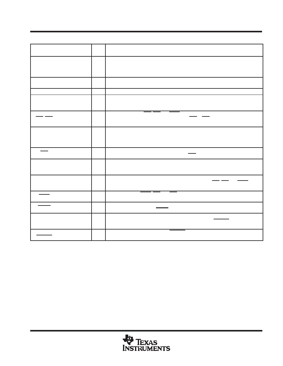
Terminal Functions
TERMINAL
I/O
DESCRIPTION
NAME
NO.
I/O
DESCRIPTION
AF/AE
24
O
Almost-full/almost-empty flag. Depth offset values can be programmed for AF/AE, or the default
value of 64 can be used for both the almost-empty offset (X) and the almost-full offset (Y). AF/AE
is high when memory contains X or less words or (512 minus Y) or more words. AF/AE is high
after reset.
D0 D17
21 14, 12 11,
9 2
I
18-bit data input port
HF
22
O
Half-full flag. HF is high when the FIFO memory contains 256 or more words. HF is low after reset.
IR
28
O
Input ready flag. IR is synchronized to the low-to-high transition of WRTCLK. When IR is low, the
FIFO is full and writes are disabled. IR is low during reset and goes high on the second low-to-high
transition of WRTCLK after reset.
OE1, OE2
56, 30
I
Output enables. When OE1, OE2, and RDEN are low and OR is high, data is read from the FIFO
on a low-to-high transition of RDCLK. When either OE1 or OE2 is high, reads are disabled and
the data outputs are in the high-impedance state.
OR
29
O
Output ready flag. OR is synchronized to the low-to-high transition of RDCLK. When OR is low,
the FIFO is empty and reads are disabled. Ready data is present on Q0 Q17 when OR is high.
OR is low during reset and goes high on the third low-to-high transition of RDCLK after the first
word is loaded to empty memory.
PEN
23
I
Program enable. After reset and before the first word is written to the FIFO, the binary value on
D0 D7 is latched as an AF/AE offset value when PEN is low and WRTCLK is high.
Q0 Q17
33 34, 36 38,
40 43, 45 49,
51, 53 55
O
18-bit data output port. After the first valid write to empty memory, the first word is output on
Q0 Q17 on the third rising edge of RDCLK. OR is also asserted high at this time to indicate ready
data. When OR is low, the last word read from the FIFO is present on Q0 Q17.
RDCLK
32
I
Read clock. RDCLK is a continuous clock and can be asynchronous or coincident to WRTCLK.
A low-to-high transition of RDCLK reads data from memory when OE1, OE2, and RDEN are low
and OR is high. OR is synchronous to the low-to-high transition of RDCLK.
RDEN
31
I
Read enable. When RDEN, OE1, and OE2 are low and OR is high, data is read from the FIFO
on the low-to-high transition of RDCLK.
RESET
1
I
Reset. To reset the FIFO, four low-to-high transitions of RDCLK and four low-to-high transitions
of WRTCLK must occur while RESET is low. This sets HF, IR, and OR low and AF/AE high.
WRTCLK
25
I
Write clock. WRTCLK is a continuous clock and can be asynchronous or coincident to RDCLK.
A low-to-high transition of WRTCLK writes data to memory when WRTEN2 is low, WRTEN1 is
high, and IR is high. IR is synchronous to the low-to-high transition of WRTCLK.
WRTEN1,
WRTEN2
27, 26
I
Write enables. When WRTEN1 is high, WRTEN2 is low, and IR is high, data is written to the FIFO
on a low-to-high transition of WRTCLK.
相關PDF資料 |
PDF描述 |
|---|---|
| SN74ALVCH16541DGGR | ALVC/VCX/A SERIES, DUAL 8-BIT DRIVER, TRUE OUTPUT, PDSO48 |
| SN74AS1008ADE4 | AS SERIES, QUAD 2-INPUT AND GATE, PDSO14 |
| SN74AS286DRE4 | AS SERIES, 9-BIT PARITY GENERATOR/CHECKER, TRUE OUTPUT, PDSO14 |
| SN74AS757NSRG4 | AS SERIES, DUAL 4-BIT DRIVER, TRUE OUTPUT, PDSO20 |
| SN74AUC1G86YZAR | AUC SERIES, 1-INPUT XOR GATE, PBGA5 |
相關代理商/技術參數(shù) |
參數(shù)描述 |
|---|---|
| SN74ALVC7804-25DL | 功能描述:先進先出 16-Bit Bus Trnscvr With 3-State Outputs RoHS:否 制造商:IDT 電路數(shù)量: 數(shù)據(jù)總線寬度:18 bit 總線定向:Unidirectional 存儲容量:4 Mbit 定時類型:Synchronous 組織:256 K x 18 最大時鐘頻率:100 MHz 訪問時間:10 ns 電源電壓-最大:3.6 V 電源電壓-最小:6 V 最大工作電流:35 mA 最大工作溫度:+ 85 C 封裝 / 箱體:TQFP-80 封裝: |
| SN74ALVC7804-25DLR | 功能描述:先進先出 512 x 18 3.3-V ASynch 先進先出 Memory RoHS:否 制造商:IDT 電路數(shù)量: 數(shù)據(jù)總線寬度:18 bit 總線定向:Unidirectional 存儲容量:4 Mbit 定時類型:Synchronous 組織:256 K x 18 最大時鐘頻率:100 MHz 訪問時間:10 ns 電源電壓-最大:3.6 V 電源電壓-最小:6 V 最大工作電流:35 mA 最大工作溫度:+ 85 C 封裝 / 箱體:TQFP-80 封裝: |
| SN74ALVC7804-40DL | 功能描述:先進先出 16-Bit Bus Trnscvr With 3-State Outputs RoHS:否 制造商:IDT 電路數(shù)量: 數(shù)據(jù)總線寬度:18 bit 總線定向:Unidirectional 存儲容量:4 Mbit 定時類型:Synchronous 組織:256 K x 18 最大時鐘頻率:100 MHz 訪問時間:10 ns 電源電壓-最大:3.6 V 電源電壓-最小:6 V 最大工作電流:35 mA 最大工作溫度:+ 85 C 封裝 / 箱體:TQFP-80 封裝: |
| SN74ALVC7804-40DLR | 功能描述:先進先出 512 x 18 3.3-V ASynch 先進先出 Memory RoHS:否 制造商:IDT 電路數(shù)量: 數(shù)據(jù)總線寬度:18 bit 總線定向:Unidirectional 存儲容量:4 Mbit 定時類型:Synchronous 組織:256 K x 18 最大時鐘頻率:100 MHz 訪問時間:10 ns 電源電壓-最大:3.6 V 電源電壓-最小:6 V 最大工作電流:35 mA 最大工作溫度:+ 85 C 封裝 / 箱體:TQFP-80 封裝: |
| SN74ALVC7805-20DL | 功能描述:先進先出 16-Bit Reg Trnscvr With 3-State Outputs RoHS:否 制造商:IDT 電路數(shù)量: 數(shù)據(jù)總線寬度:18 bit 總線定向:Unidirectional 存儲容量:4 Mbit 定時類型:Synchronous 組織:256 K x 18 最大時鐘頻率:100 MHz 訪問時間:10 ns 電源電壓-最大:3.6 V 電源電壓-最小:6 V 最大工作電流:35 mA 最大工作溫度:+ 85 C 封裝 / 箱體:TQFP-80 封裝: |
發(fā)布緊急采購,3分鐘左右您將得到回復。