- 您現(xiàn)在的位置:買賣IC網(wǎng) > PDF目錄373427 > SMJ44400 (Electronic Theatre Controls, Inc.) 1M x 4 DRAM DYNAMIC RANDOM-ACCESS MEMORY PDF資料下載
參數(shù)資料
| 型號: | SMJ44400 |
| 廠商: | Electronic Theatre Controls, Inc. |
| 英文描述: | 1M x 4 DRAM DYNAMIC RANDOM-ACCESS MEMORY |
| 中文描述: | 100萬× 4的DRAM動態(tài)隨機(jī)存取存儲器 |
| 文件頁數(shù): | 5/21頁 |
| 文件大?。?/td> | 351K |
| 代理商: | SMJ44400 |
DRAM
SMJ44400
Austin Semiconductor, Inc.
SMJ44400
Rev. 2.0 10/01
Austin Semiconductor, Inc. reserves the right to change products or specifications without notice.
5
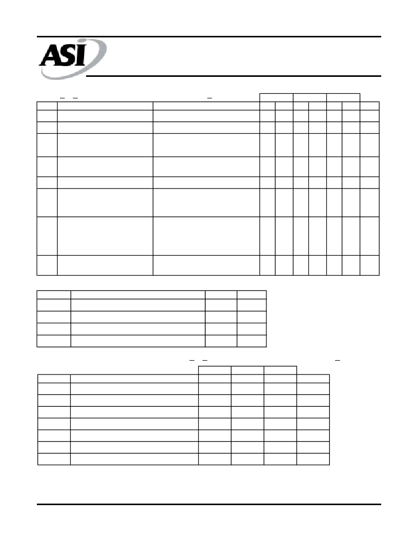
SYM
V
OH
High-level output voltage
V
OL
Low-level output voltage
PARAMETER
TEST CONDITIONS
I
OH
= -5mA
I
OL
= 4.2mA
V
CC
= 5.5V, V
I
= 0V to 6.5V, All
other pins = 0V to V
CC
V
CC
= 5.5V, V
O
= 0V to V
CC,
CAS\ High
V
CC
= 5.5V, Minimum cycle
After 1 memory cycle,
RAS\ and CAS\ High,
V
IH
= 2.4V
MIN MAX MIN MAX MIN MAX UNIT
2.4
2.4
2.4
V
0.4
0.4
0.4
V
I
I
Input current (leakage)
±10
±10
±10
μA
I
O
Output current (leakage)
±10
±10
±10
μA
I
CC1
Read - or write-cycle current
1
85
80
70
mA
I
CC2
Standby current
4
4
4
mA
I
CC3
Average refresh current
(RAS\ only, or CBR\)
1
V
CC
= 5.5V, Minimum cycle,
RAS\ cycling,
CAS\ High (RAS\ only),
RAS\ Low after CAS\ Low (CBR)
85
75
65
mA
I
CC4
Average page current
2
V
CC
= 5.5V, t
PC
= minimum,
RAS\ Low, CAS\ cycling
50
40
35
mA
-8
-10
-12
ELECTRICAL CHARACTERISTICS AND RECOMMENDED OPERATING CONDITIONS
(-55
o
C<T
A
<125
o
C or -40
o
C to +85
o
C; Vcc = 5V +10%)
NOTES:
1. Measured with a maximum of one address change while RAS\ = V
IL
.
2. Measured with a maximum of one address change while CAS\ = V
IH
.
3. V
CC
= 5V ±0.5V and the bias on the pins under test is 0V. Capacitance is sampled only at initial design and after any major change.
4. t
OFF
and t
OEZ
are specified when the output is no longer driven. The outputs are disabled by bringing either OE\ or CAS\ High.
CAPACITANCE (f = 1MHz)
3
SYM
C
i(A)
Input capacitance, address inputs
C
i(RC)
Input capacitance, strobe inputs
C
i(W)
Input capacitance, write-enable inputs
C
O
Output capacitance
PARAMETER
MAX
7
UNIT
pF
10
pF
10
pF
10
pF
SWITCHING CHARACTERISTICS
(-55
o
C<T
A
<125
o
C or -40
o
C to +85
o
C; Vcc = 5V +10%)
-8
-10
MAX
45
-12
MAX
55
SYM
t
AA
t
CAC
t
CPA
t
RAC
t
OEA
t
OFF
t
OEZ
PARAMETERS
MAX
40
UNIT
ns
Access time from column address
Access time from CAS\ low
20
25
30
ns
Access time from column precharge
45
50
55
ns
Access time from RAS\ low
80
100
120
ns
Access time from OE\ low
Output disable time after CAS\ High
4
Output disable tiem after OE\ High
4
20
25
30
ns
20
25
30
ns
20
25
30
ns
相關(guān)PDF資料 |
PDF描述 |
|---|---|
| SMJ44400HR | 1M x 4 DRAM DYNAMIC RANDOM-ACCESS MEMORY |
| SMJ44400JD | 1M x 4 DRAM DYNAMIC RANDOM-ACCESS MEMORY |
| SMJ44C251B | 262144 BY 4-BIT MULTIPORT VIDEO RAM |
| SMJ4C1024-10HJ | 1048576 BY 1-BIT DYNAMIC RANDOM-ACCESS MEMORY |
| SMJ4C1024-10HK | 1048576 BY 1-BIT DYNAMIC RANDOM-ACCESS MEMORY |
相關(guān)代理商/技術(shù)參數(shù) |
參數(shù)描述 |
|---|---|
| SMJ44400-10HMM | 制造商:Rochester Electronics LLC 功能描述:- Bulk |
| SMJ44400-80HMM | 制造商:Rochester Electronics LLC 功能描述:- Bulk |
| SMJ44400-80JDM | 制造商:Micross Components 功能描述:1M X 4 DRAM - Bulk |
| SMJ44400HR | 制造商:未知廠家 制造商全稱:未知廠家 功能描述:1M x 4 DRAM DYNAMIC RANDOM-ACCESS MEMORY |
| SMJ44400JD | 制造商:未知廠家 制造商全稱:未知廠家 功能描述:1M x 4 DRAM DYNAMIC RANDOM-ACCESS MEMORY |
發(fā)布緊急采購,3分鐘左右您將得到回復(fù)。