- 您現(xiàn)在的位置:買賣IC網(wǎng) > PDF目錄98083 > SM320F2812HFGM (TEXAS INSTRUMENTS INC) 16-BIT, 150 MHz, OTHER DSP, CQFP172 PDF資料下載
參數(shù)資料
| 型號: | SM320F2812HFGM |
| 廠商: | TEXAS INSTRUMENTS INC |
| 元件分類: | 數(shù)字信號處理 |
| 英文描述: | 16-BIT, 150 MHz, OTHER DSP, CQFP172 |
| 封裝: | NCTB, CERAMIC, QFP-172 |
| 文件頁數(shù): | 138/147頁 |
| 文件大小: | 1721K |
| 代理商: | SM320F2812HFGM |
第1頁第2頁第3頁第4頁第5頁第6頁第7頁第8頁第9頁第10頁第11頁第12頁第13頁第14頁第15頁第16頁第17頁第18頁第19頁第20頁第21頁第22頁第23頁第24頁第25頁第26頁第27頁第28頁第29頁第30頁第31頁第32頁第33頁第34頁第35頁第36頁第37頁第38頁第39頁第40頁第41頁第42頁第43頁第44頁第45頁第46頁第47頁第48頁第49頁第50頁第51頁第52頁第53頁第54頁第55頁第56頁第57頁第58頁第59頁第60頁第61頁第62頁第63頁第64頁第65頁第66頁第67頁第68頁第69頁第70頁第71頁第72頁第73頁第74頁第75頁第76頁第77頁第78頁第79頁第80頁第81頁第82頁第83頁第84頁第85頁第86頁第87頁第88頁第89頁第90頁第91頁第92頁第93頁第94頁第95頁第96頁第97頁第98頁第99頁第100頁第101頁第102頁第103頁第104頁第105頁第106頁第107頁第108頁第109頁第110頁第111頁第112頁第113頁第114頁第115頁第116頁第117頁第118頁第119頁第120頁第121頁第122頁第123頁第124頁第125頁第126頁第127頁第128頁第129頁第130頁第131頁第132頁第133頁第134頁第135頁第136頁第137頁當前第138頁第139頁第140頁第141頁第142頁第143頁第144頁第145頁第146頁第147頁
Electrical Specifications
90
December 2004
SGUS053
6.9
Timing Parameter Symbology
Timing parameter symbols used are created in accordance with JEDEC Standard 100. To shorten the
symbols, some of the pin names and other related terminology have been abbreviated as follows:
Lowercase subscripts and their meanings:
Letters and symbols and their meanings:
a
access time
H
High
c
cycle time (period)
L
Low
d
delay time
V
Valid
f
fall time
X
Unknown, changing, or don’t care level
h
hold time
Z
High impedance
r
rise time
su
setup time
t
transition time
v
valid time
w
pulse duration (width)
6.10
General Notes on Timing Parameters
All output signals from the 28x devices (including XCLKOUT) are derived from an internal clock such that all
output transitions for a given half-cycle occur with a minimum of skewing relative to each other.
The signal combinations shown in the following timing diagrams may not necessarily represent actual cycles.
For actual cycle examples, see the appropriate cycle description section of this document.
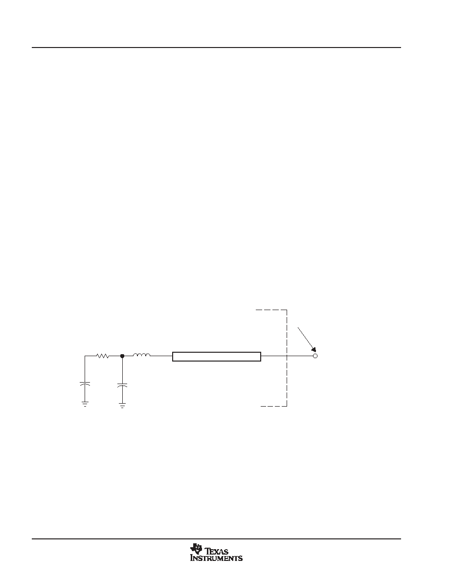
6.11
Test Load Circuit
This test load circuit is used to measure all switching characteristics provided in this document.
Transmission Line
4.0 pF
1.85 pF
Z0 = 50
(see note)
Tester Pin Electronics
Data Sheet Timing Reference Point
Output
Under
Test
NOTE: The data sheet provides timing at the device pin. For output timing analysis, the tester pin electronics and its transmission line effects
must be taken into account. A transmission line with a delay of 2 ns or longer can be used to produce the desired transmission line effect.
The transmission line is intended as a load only. It is not necessary to add or subtract the transmission line delay (2 ns or longer) from
the data sheet timing.
42
3.5 nH
Device Pin
(see note)
Input requirements in this data sheet are tested with an input slew rate of < 4 Volts per nanosecond (4 V/ns) at the device pin.
Figure 66. 3.3-V Test Load Circuit
相關PDF資料 |
PDF描述 |
|---|---|
| SM320MCM41DHFHM40 | 32-BIT, 40 MHz, OTHER DSP, CQFP352 |
| SM320MCM42CHFNM40 | 32-BIT, 40 MHz, OTHER DSP, CQFP408 |
| SM320VC33HFGM150 | 32-BIT, 75 MHz, OTHER DSP, CQFP164 |
| SM34020AHTM32 | GRAPHICS PROCESSOR, CQFP132 |
| SM563 | 4-BIT, MROM, MICROCONTROLLER, PQFP64 |
相關代理商/技術(shù)參數(shù) |
參數(shù)描述 |
|---|---|
| SM320F2812HFGM150 | 功能描述:數(shù)字信號處理器和控制器 - DSP, DSC Military DSP RoHS:否 制造商:Microchip Technology 核心:dsPIC 數(shù)據(jù)總線寬度:16 bit 程序存儲器大小:16 KB 數(shù)據(jù) RAM 大小:2 KB 最大時鐘頻率:40 MHz 可編程輸入/輸出端數(shù)量:35 定時器數(shù)量:3 設備每秒兆指令數(shù):50 MIPs 工作電源電壓:3.3 V 最大工作溫度:+ 85 C 封裝 / 箱體:TQFP-44 安裝風格:SMD/SMT |
| SM320F2812HFGS150 | 功能描述:數(shù)字信號處理器和控制器 - DSP, DSC HT Dig Signal Controller RoHS:否 制造商:Microchip Technology 核心:dsPIC 數(shù)據(jù)總線寬度:16 bit 程序存儲器大小:16 KB 數(shù)據(jù) RAM 大小:2 KB 最大時鐘頻率:40 MHz 可編程輸入/輸出端數(shù)量:35 定時器數(shù)量:3 設備每秒兆指令數(shù):50 MIPs 工作電源電壓:3.3 V 最大工作溫度:+ 85 C 封裝 / 箱體:TQFP-44 安裝風格:SMD/SMT |
| SM320F2812-HT | 制造商:TI 制造商全稱:Texas Instruments 功能描述:Digital Signal Processor |
| SM320F2812KGDS150A | 功能描述:數(shù)字信號處理器和控制器 - DSP, DSC HT Dig Signal Controller RoHS:否 制造商:Microchip Technology 核心:dsPIC 數(shù)據(jù)總線寬度:16 bit 程序存儲器大小:16 KB 數(shù)據(jù) RAM 大小:2 KB 最大時鐘頻率:40 MHz 可編程輸入/輸出端數(shù)量:35 定時器數(shù)量:3 設備每秒兆指令數(shù):50 MIPs 工作電源電壓:3.3 V 最大工作溫度:+ 85 C 封裝 / 箱體:TQFP-44 安裝風格:SMD/SMT |
| SM320F2812PGFMEP | 功能描述:數(shù)字信號處理器和控制器 - DSP, DSC EP Digital Signal Proc RoHS:否 制造商:Microchip Technology 核心:dsPIC 數(shù)據(jù)總線寬度:16 bit 程序存儲器大小:16 KB 數(shù)據(jù) RAM 大小:2 KB 最大時鐘頻率:40 MHz 可編程輸入/輸出端數(shù)量:35 定時器數(shù)量:3 設備每秒兆指令數(shù):50 MIPs 工作電源電壓:3.3 V 最大工作溫度:+ 85 C 封裝 / 箱體:TQFP-44 安裝風格:SMD/SMT |
發(fā)布緊急采購,3分鐘左右您將得到回復。