- 您現(xiàn)在的位置:買(mǎi)賣(mài)IC網(wǎng) > PDF目錄368623 > SI91861DY (Vishay Intertechnology,Inc.) 400-mA Smart Regulator for Network Interface Card PDF資料下載
參數(shù)資料
| 型號(hào): | SI91861DY |
| 廠商: | Vishay Intertechnology,Inc. |
| 英文描述: | 400-mA Smart Regulator for Network Interface Card |
| 中文描述: | 400毫安智能調(diào)節(jié)器的網(wǎng)絡(luò)接口卡 |
| 文件頁(yè)數(shù): | 2/7頁(yè) |
| 文件大小: | 109K |
| 代理商: | SI91861DY |
Si91861
Vishay Siliconix
www.vishay.com
2
Document Number: 71637
S-40702—Rev. B, 19-Apr-04
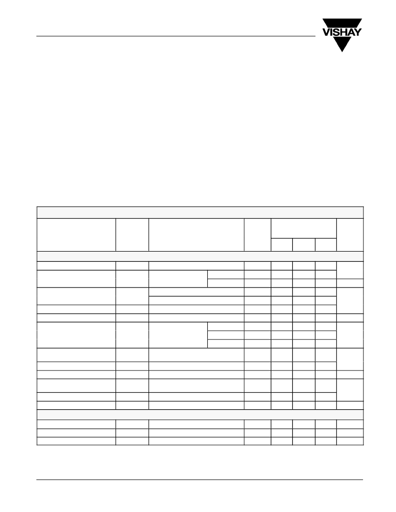
ABSOLUTE MAXIMUM RATINGS
Pin 2, 4 Voltage
Linear Regulator Output Current
Bypass Switch Current
Maximum Junction Temperature, T
J(max)
Storage Temperature, T
STG
ESD (Human Body Model)
0.3 V to 6 V
600 mA
600 mA
150 C
55 C to 150 C
. . . . . . . . . . . . . . . . . . . . . . . . . . . . . . . . . . . . . . . .
. . . . . . . . . . . . . . . . . . . . . . . . . . . . . . .
. . . . . . . . . . . . . . . . . . . . . . . . . . . . . . . . . . . . . . .
. . . . . . . . . . . . . . . . . . . . . . . .
. . . . . . . . . . . . . . . . . . . . . . . . . .
. . . . . . . . . . . . . . . . . . . . . . . . . . . . . . . . . . . . . . .
2 kV
Package Power Dissipation
b
P
D
. . . . . . . . . . . . . . . . . . . . . . . .
Thermal Impedance (
JA
)
a
Notes
a.
Device mounted with all leads soldered or welded to PC board.
b.
Derate 16 mW/ C above T
A
= 25 C
2W (internally limited via thermal shutdown)
62.5 C/W
. . . . . . . . . . . . . . . . . . . . . . . . . . . . . . . . . .
Stresses beyond those listed under “Absolute Maximum Ratings” may cause permanent damage to the device. These are stress ratings only, and functional operation
of the device at these or any other conditions beyond those indicated in the operational sections of the specifications is not implied. Exposure to absolute maximum
rating conditions for extended periods may affect device reliability.
RECOMMENDED OPERATING RANGE
5-V
IN
3.3-V
AUX
4.5 V to 5.5 V
3 V to 3.6 V
. . . . . . . . . . . . . . . . . . . . . . . . . . . . . . . . . . . . . . . . . . . . . . . . .
. . . . . . . . . . . . . . . . . . . . . . . . . . . . . . . . . . . . . . . . . . . . . . .
3.3 V
OUT
Loading
Operating Ambient Temperature, T
A
1 mA to 400 mA
40 C to 85 C
. . . . . . . . . . . . . . . . . . . . . . . . . . . . . . . . . . .
. . . . . . . . . . . . . . . . . . . .
SPECIFICATIONS
Test Conditions
Unless Otherwise Specified
5 V 5 V 3 3 V
= 5 V, 3.3 V
AUX
= 3.3 V
I
OUT
= 1 mA, C
IN
= 4.7 F, C
OUT
= 2.2 F
3 3 V
Limits
40 to 85 C
Parameter
Symbol
Temp
a
Min
b
Typ
c
Max
b
Unit
Regulator Mode
Output Voltage (Regulator)
V
O(reg)
0 mA < I
OUT
< 400 mA, 5 V
IN
4.5 V
Full
3.201
3.3
3.399
V
5 V
IN
Select
Rising Edge of Hysteresis
Threshold
Full
4.30
4.475
Hysteresis
Full
230
mV
Ground Pin Current
In Regulator Mode
d
I
GND
I
O
= 0 mA
Full
0.3
0.8
I
O
= 400 mA
Full
0.7
1.6
mA
Peak Output Current (Regulator)
I
O
t
PW
= 2 ms
Full
600
Output Noise Voltage (Regulator)
e
N
BW = 50 Hz to100 kHz, I
OUT
= 150 mA
Room
300
V
rms
3 3 V
3.3 V
OUT
V
IN
1 kHz
Room
60
Ripple Rejection (Regulator)
I
= 150 mA
OUT
10 kHz
Room
40
dB
100 kHz
Room
30
Dynamic Line Regulation
V
O(line)
V
= 4.5 V
t
R
/t
F
= 2 s, I
OUT
= 150 mA
5.5 V
Room
10
mV
Dynamic Load Regulation
V
O(load)
t
ON
I
OUT
: 1 mA to 150 mA, t
R
/t
F
= 2 s
Room
20
V
OUT
Turn-On-Time
Room
15
s
Thermal Shutdown Junction
Temperature
T
J(sd)
Full
165
C
Thermal Hysteresis
T
HYST
Full
20
Short Circuit Current
I
SC
3.3 V
OUT
= 0 V
Room
900
mA
Bypass Mode (5 V
IN
= GND)
Output Voltage
V
O(BP)
r
DS(on)
I
GND
0 mA < I
OUT
< 150 mA
3.0 V
V
AUX
0 mA < I
OUT
< 400 mA
Full
3.247
V
Bypass Switch On-Resistance
3.6 V
Full
0.2
0.35
Ground Current
d
Full
200
400
A
Notes
a.
b.
c.
d.
Room = 25 C, Full =
40 to 85 C.
The algebraic convention whereby the most negative value is a minimum and the most positive a maximum.
Typical values are for DESIGN AID ONLY, not guaranteed nor subject to production testing. Typical values at 25 C ambient.
Ground pin current includes the IC supply current and the current to drive the linear regulator or bypass switch.
相關(guān)PDF資料 |
PDF描述 |
|---|---|
| SI91861DY-T1 | 400-mA Smart Regulator for Network Interface Card |
| SI91861DY-T1-E3 | 400-mA Smart Regulator for Network Interface Card |
| SI9400DY | P-Channel 20-V (D-S) MOSFET, Low-Threshold |
| SI9433DY | P-Channel 20-V (D-S) MOSFET, Low-Threshold |
| Si9433BDY-E3 | P-Channel 20-V (D-S) MOSFET, Low-Threshold |
相關(guān)代理商/技術(shù)參數(shù) |
參數(shù)描述 |
|---|---|
| SI91861DY-T1 | 功能描述:低壓差穩(wěn)壓器 - LDO 400mA 3.3V Smart LDO w/Bypass RoHS:否 制造商:Texas Instruments 最大輸入電壓:36 V 輸出電壓:1.4 V to 20.5 V 回動(dòng)電壓(最大值):307 mV 輸出電流:1 A 負(fù)載調(diào)節(jié):0.3 % 輸出端數(shù)量: 輸出類(lèi)型:Fixed 最大工作溫度:+ 125 C 安裝風(fēng)格:SMD/SMT 封裝 / 箱體:VQFN-20 |
| SI91861DY-T1-E3 | 功能描述:低壓差穩(wěn)壓器 - LDO 400mA 3.3V Smart LDO w/Bypass RoHS:否 制造商:Texas Instruments 最大輸入電壓:36 V 輸出電壓:1.4 V to 20.5 V 回動(dòng)電壓(最大值):307 mV 輸出電流:1 A 負(fù)載調(diào)節(jié):0.3 % 輸出端數(shù)量: 輸出類(lèi)型:Fixed 最大工作溫度:+ 125 C 安裝風(fēng)格:SMD/SMT 封裝 / 箱體:VQFN-20 |
| SI91871 | 制造商:VISHAY 制造商全稱(chēng):Vishay Siliconix 功能描述:300-mA Ultra Low-Noise LDO Regulator With Discharge Option |
| SI91871_05 | 制造商:VISHAY 制造商全稱(chēng):Vishay Siliconix 功能描述:300-mA Ultra Low-Noise LDO Regulator With Discharge Option |
| SI91871DMP-12-E3 | 功能描述:低壓差穩(wěn)壓器 - LDO 300mA LDO 1.2V w/Discharge Option RoHS:否 制造商:Texas Instruments 最大輸入電壓:36 V 輸出電壓:1.4 V to 20.5 V 回動(dòng)電壓(最大值):307 mV 輸出電流:1 A 負(fù)載調(diào)節(jié):0.3 % 輸出端數(shù)量: 輸出類(lèi)型:Fixed 最大工作溫度:+ 125 C 安裝風(fēng)格:SMD/SMT 封裝 / 箱體:VQFN-20 |
發(fā)布緊急采購(gòu),3分鐘左右您將得到回復(fù)。