- 您現在的位置:買賣IC網 > PDF目錄373395 > Si4133G-BT* (Electronic Theatre Controls, Inc.) DUAL-BAND RF SYNTHESIZER WITH INTEGRATED VCOS FOR GSM AND GPRS WIRELESS COMMUNICATIONS PDF資料下載
參數資料
| 型號: | Si4133G-BT* |
| 廠商: | Electronic Theatre Controls, Inc. |
| 英文描述: | DUAL-BAND RF SYNTHESIZER WITH INTEGRATED VCOS FOR GSM AND GPRS WIRELESS COMMUNICATIONS |
| 中文描述: | 雙波段射頻合成器集成的GSM和GPRS無線通訊和VCO |
| 文件頁數: | 18/32頁 |
| 文件大小: | 466K |
第1頁第2頁第3頁第4頁第5頁第6頁第7頁第8頁第9頁第10頁第11頁第12頁第13頁第14頁第15頁第16頁第17頁當前第18頁第19頁第20頁第21頁第22頁第23頁第24頁第25頁第26頁第27頁第28頁第29頁第30頁第31頁第32頁
Si4133G
18
Rev. 1.1
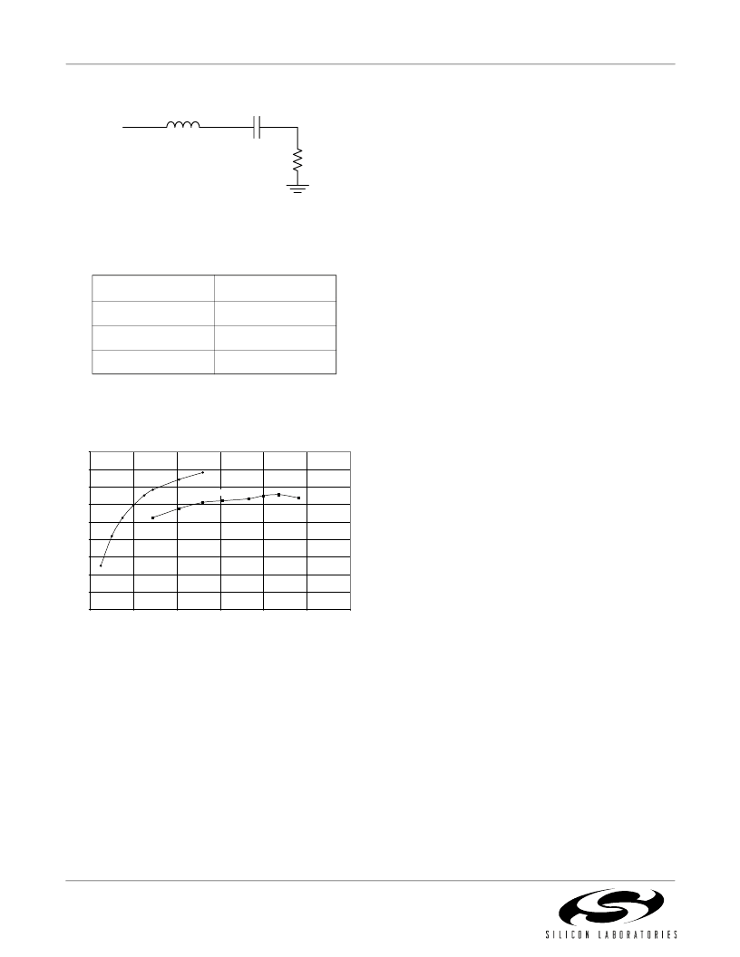
Figure 17. IFOUT 50
Test Circuit
The IF output level is dependent upon the load.
Figure 18 displays the output level versus load
resistance for a variety of output frequencies.
Figure 18. Typical IF Output Voltage vs. Load
Resistance at 550 MHz
For resistive loads greater than 500
the output level
saturates and the bias currents in the IF output amplifier
are higher than they need be. The LPWR bit in the Main
Configuration register (Register 0) can be set to 1 to
reduce the bias currents and therefore reduce the
power dissipated by the IF amplifier. For loads less than
500
LPWR should be set to 0 to maximize the output
level.
Reference Frequency Amplifier
The Si4133G provides a reference frequency amplifier.
If the driving signal has CMOS levels it can be
connected directly to the XIN pin. Otherwise, the
reference frequency signal should be AC coupled to the
XIN pin through a 560 pF capacitor.
Power Down Modes
Table 9 summarizes the power down functionality. The
Si4133G can be powered down by taking the PWDNB
pin low or by setting bits in the Power Down register
(Register 1). When the PWDNB pin is low, the Si4133G
will be powered down regardless of the Power Down
register settings. When the PWDNB pin is high, power
management is under control of the Power Down
register bits.
The reference frequency amplifier, IF, and RF sections
of the Si4133G circuitry can be individually powered
down by setting the Power Down register bits PDIB and
PDRB low, respectively. The reference frequency
amplifier will also be powered up if either of the PDRB
or PDIB bits are high. Also, setting the AUTOPDB bit to
1 in the Main Configuration register (Register 0) is
equivalent to setting both bits in the Power Down
register to 1. The serial interface remains available and
can be written in all power down modes.
Auxiliary Output (AUXOUT)
The signal appearing on AUXOUT is selected by setting
the AUXSEL bits in the Main Configuration register
(Register 0).
The LDETB signal can be selected by setting the
AUXSEL bits to 11. As discussed previously, this signal
can be used to indicate that the IF or RF PLL is about to
lose lock due to excessive ambient temperature drift and
should be re-tuned.
Table 8. L
MATCH
Values
Frequency
L
MATCH
500–600 MHz
40 nH
600–800 MHz
27 nH
800–1 GHz
18 nH
IFOUT
L
MATCH
560 pF
50
0
50
100
150
200
250
300
350
400
450
0
200
400
600
800
1000
1200
Load Resistance (
)
O
LPWR=0
LPWR=1
相關PDF資料 |
PDF描述 |
|---|---|
| Si4123G | DUAL-BAND RF SYNTHESIZER WITH INTEGRATED VCOS FOR GSM AND GPRS WIRELESS COMMUNICATIONS |
| Si4133G | DUAL-BAND RF SYNTHESIZER WITH INTEGRATED VCOS FOR GSM AND GPRS WIRELESS COMMUNICATIONS |
| Si4112G | DUAL-BAND RF SYNTHESIZER WITH INTEGRATED VCOS FOR GSM AND GPRS WIRELESS COMMUNICATIONS |
| Si4112G-BM | DUAL-BAND RF SYNTHESIZER WITH INTEGRATED VCOS FOR GSM AND GPRS WIRELESS COMMUNICATIONS |
| Si4113G | DUAL-BAND RF SYNTHESIZER WITH INTEGRATED VCOS FOR GSM AND GPRS WIRELESS COMMUNICATIONS |
相關代理商/技術參數 |
參數描述 |
|---|---|
| SI4133G-X2 | 制造商:未知廠家 制造商全稱:未知廠家 功能描述:DUAL-BAND RF SYNTHESIZER WITH INTEGRATED VCOS FOR GSM AND GPRS WIRELESS COMMUNICATIONS |
| SI4133GX2-BM | 功能描述:射頻無線雜項 Dual-Band Synthesizer RoHS:否 制造商:Texas Instruments 工作頻率:112 kHz to 205 kHz 電源電壓-最大:3.6 V 電源電壓-最小:3 V 電源電流:8 mA 最大功率耗散: 工作溫度范圍:- 40 C to + 110 C 封裝 / 箱體:VQFN-48 封裝:Reel |
| SI4133GX2M-EVB | 功能描述:射頻開發(fā)工具 Dual-Band GSM RoHS:否 制造商:Taiyo Yuden 產品:Wireless Modules 類型:Wireless Audio 工具用于評估:WYSAAVDX7 頻率: 工作電源電壓:3.4 V to 5.5 V |
| SI4133G-XM2 | 制造商:未知廠家 制造商全稱:未知廠家 功能描述:DUAL-BAND RF SYNTHESIZER WITH INTEGRATED VCOS FOR GSM AND GPRS WIRELESS COMMUNICATIONS |
發(fā)布緊急采購,3分鐘左右您將得到回復。