- 您現(xiàn)在的位置:買賣IC網(wǎng) > PDF目錄373395 > Si3200-X-GS (Electronic Theatre Controls, Inc.) DUAL PROGRAMMABLE CMOS SLIC WITH LINE MONITORING PDF資料下載
參數(shù)資料
| 型號: | Si3200-X-GS |
| 廠商: | Electronic Theatre Controls, Inc. |
| 英文描述: | DUAL PROGRAMMABLE CMOS SLIC WITH LINE MONITORING |
| 中文描述: | 兩個可編程的CMOS用戶接口與在線監(jiān)測 |
| 文件頁數(shù): | 39/128頁 |
| 文件大小: | 2327K |
| 代理商: | SI3200-X-GS |
第1頁第2頁第3頁第4頁第5頁第6頁第7頁第8頁第9頁第10頁第11頁第12頁第13頁第14頁第15頁第16頁第17頁第18頁第19頁第20頁第21頁第22頁第23頁第24頁第25頁第26頁第27頁第28頁第29頁第30頁第31頁第32頁第33頁第34頁第35頁第36頁第37頁第38頁當(dāng)前第39頁第40頁第41頁第42頁第43頁第44頁第45頁第46頁第47頁第48頁第49頁第50頁第51頁第52頁第53頁第54頁第55頁第56頁第57頁第58頁第59頁第60頁第61頁第62頁第63頁第64頁第65頁第66頁第67頁第68頁第69頁第70頁第71頁第72頁第73頁第74頁第75頁第76頁第77頁第78頁第79頁第80頁第81頁第82頁第83頁第84頁第85頁第86頁第87頁第88頁第89頁第90頁第91頁第92頁第93頁第94頁第95頁第96頁第97頁第98頁第99頁第100頁第101頁第102頁第103頁第104頁第105頁第106頁第107頁第108頁第109頁第110頁第111頁第112頁第113頁第114頁第115頁第116頁第117頁第118頁第119頁第120頁第121頁第122頁第123頁第124頁第125頁第126頁第127頁第128頁
Si3232
Preliminary Rev. 0.96
39
In addition to the variable frequency and amplitude,
there is a selectable dc offset (V
OFF
) that can be added
to the waveform. The dc offset is defined in the RINGOF
RAM location. The ringing generator has two timers
which allow on/off cadence settings up to 8 s on/8 s off.
In addition to controlling ringing cadence, these timers
control the transition into and out of the ringing state.
To initiate ringing, the user must program the
RINGFREQ,
RINGAMP,
addresses as well as the RINGTA, and RINGTI
registers, and select the ringing waveshape and dc
offset. Once this is done, the TAEN and TIEN bits are
set as desired. Ringing state is invoked by a write to the
linefeed register. At the expiration of RINGTA, the
Si3232 turns off the ringing waveform and goes to the
on-hook transmission state. At the expiration of RINGTI,
ringing is initiated again. This process continues as long
as the two timers are enabled and the linefeed register
remains in the ringing state.
4.6.2. Internal Trapezoidal Ringing
In addition to the traditional sinusoidal ringing
waveform, the Si3232 can generate a trapezoidal
ringing waveform similar to the one illustrated in
Figure 19.
The
RINGFREQ,
RINGPHAS RAM locations are used for programming
the ringing wave shape as follows:
RINGPHAS = 4 x Period x 8000
RINGAMP = (Desired V/160.8 V) x (2
15
)
RINGFREQ = (2 x RINGAMP) / (t
RISE
x 8000)
RINGFREQ is a value that is added or subtracted from
the waveform to ramp the signal up or down in a linear
fashion. This value is a function of rise time, period, and
amplitude, where rise time and period are related
through the following equation for the crest factor of a
trapezoidal waveform.
and
RINGPHAS
RAM
RINGAMP,
and
where
So, for a 90 V
PK
, 20 Hz trapezoidal waveform with a
crest factor of 1.3, the period is 0.05 s, and the rise time
requirement is 0.015 s.
RINGPHAS = 4 x 0.05 x 8000 = 1600 (0x0640)
RINGAMP = 90/160.8 x (2
15
) = 18340 (0x47A5)
RINGFREQ = (2 x RINGAMP) (0.0153 x 8000) =
300 (0x012C)
The time registers and interrupts described in the
sinusoidal ring description also apply to the trapezoidal
ring waveform.
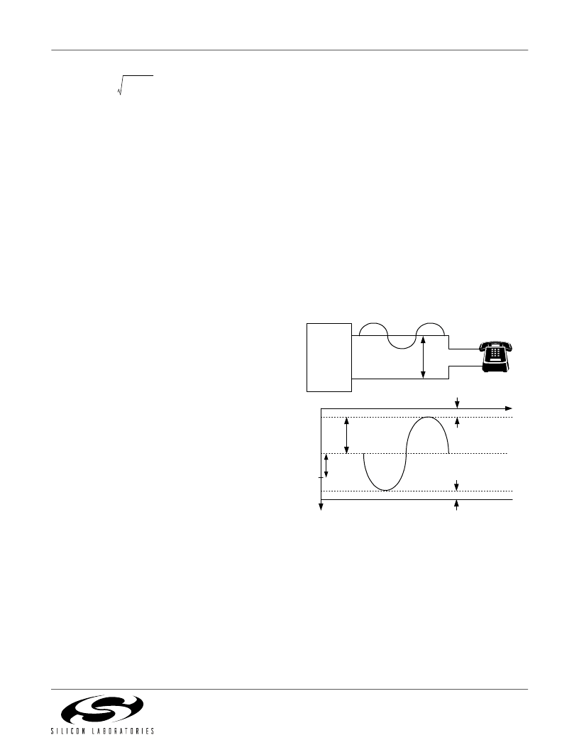
4.7. Internal Unbalanced Ringing
The Si3232 also provides the ability to generate a
traditional battery-backed unbalanced ringing waveform
for ringing terminating devices that require a high dc
content or for use in ground-start systems that cannot
tolerate a ringing waveform on both the TIP and RING
leads. The unbalanced ringing scheme applies the
ringing signal to the RING lead; the TIP lead remains at
the programmed VCM voltage that is very close to
ground. A programmable dc offset can be preset to
provide dc current for ring trip detection. Figure 18
illustrates the internal unbalanced ringing waveform.
Figure 18. Internal Unbalanced Ringing
To enable unbalanced ringing, set the RINGUNB bit of
the RINGCON register. As is the case with internal
balanced ringing, the unbalanced ringing waveform is
generated by using the on-chip ringing tone generator.
The tone generator used to generate ringing tones is a
two-pole resonator with programmable frequency and
amplitude. Since ringing frequencies are low compared
to the audio band signaling frequencies, the ringing
waveform is generated at a 1 kHz rate.
The ringing generator is programmed via the RINGAMP,
RINGFREQ, and RINGPHAS registers. The RINGOF
register is used to set the dc offset position around
RINGAMP
1
4
--
00789
1.99211
.
2
15
(
)
×
160.173
---------------------
×
273
0x111
=
=
=
t
RISE
3
4
--
T 1
CF
2
----------
–
=
T
Period
f
RING
--------------
CF
desired crest factor
=
=
=
RING
TIP
V
RING
Si3232
DC Offset
GND
V
TIP
V
RING
V
BATR
-80V
V
OVRING
V
CM
DC Offset
V
OFF
相關(guān)PDF資料 |
PDF描述 |
|---|---|
| Si3232-X-FQ | DUAL PROGRAMMABLE CMOS SLIC WITH LINE MONITORING |
| Si3232-X-GQ | DUAL PROGRAMMABLE CMOS SLIC WITH LINE MONITORING |
| SI3211 | PROSLIC PROGRAMMABLE CMOS SLIC/CODEC WITH RINGING/BATTERY VOLTAGE GENERATION |
| SI3210M-KT | PROSLIC PROGRAMMABLE CMOS SLIC/CODEC WITH RINGING/BATTERY VOLTAGE GENERATION |
| SI3210M-BT | PROSLIC PROGRAMMABLE CMOS SLIC/CODEC WITH RINGING/BATTERY VOLTAGE GENERATION |
相關(guān)代理商/技術(shù)參數(shù) |
參數(shù)描述 |
|---|---|
| Si3201-BS | 功能描述:電信線路管理 IC 100V Linefeed Inter- face IC for Si321x RoHS:否 制造商:STMicroelectronics 產(chǎn)品:PHY 接口類型:UART 電源電壓-最大:18 V 電源電壓-最小:8 V 電源電流:30 mA 最大工作溫度:+ 85 C 最小工作溫度:- 40 C 安裝風(fēng)格:SMD/SMT 封裝 / 箱體:VFQFPN-48 封裝:Tray |
| SI3201-BSR | 制造商:Silicon Laboratories Inc 功能描述: |
| Si3201-FS | 功能描述:電信線路管理 IC 100 V Linefeed InterfaceICSi321X RoHS:否 制造商:STMicroelectronics 產(chǎn)品:PHY 接口類型:UART 電源電壓-最大:18 V 電源電壓-最小:8 V 電源電流:30 mA 最大工作溫度:+ 85 C 最小工作溫度:- 40 C 安裝風(fēng)格:SMD/SMT 封裝 / 箱體:VFQFPN-48 封裝:Tray |
| SI3201-FSR | 功能描述:電信線路管理 IC 100 V Linefeed Interface RoHS:否 制造商:STMicroelectronics 產(chǎn)品:PHY 接口類型:UART 電源電壓-最大:18 V 電源電壓-最小:8 V 電源電流:30 mA 最大工作溫度:+ 85 C 最小工作溫度:- 40 C 安裝風(fēng)格:SMD/SMT 封裝 / 箱體:VFQFPN-48 封裝:Tray |
| Si3201-GS | 功能描述:電信線路管理 IC 100V Linefeed Inter- face IC for Si321x RoHS:否 制造商:STMicroelectronics 產(chǎn)品:PHY 接口類型:UART 電源電壓-最大:18 V 電源電壓-最小:8 V 電源電流:30 mA 最大工作溫度:+ 85 C 最小工作溫度:- 40 C 安裝風(fēng)格:SMD/SMT 封裝 / 箱體:VFQFPN-48 封裝:Tray |
發(fā)布緊急采購,3分鐘左右您將得到回復(fù)。