- 您現(xiàn)在的位置:買賣IC網(wǎng) > PDF目錄376339 > SCAN90CP02SP (NATIONAL SEMICONDUCTOR CORP) Product Description:Scotch-Brite Ultra Heavy Duty Hand Pad, Tan RoHS Compliant: NA PDF資料下載
參數(shù)資料
| 型號: | SCAN90CP02SP |
| 廠商: | NATIONAL SEMICONDUCTOR CORP |
| 元件分類: | 運動控制電子 |
| 英文描述: | Product Description:Scotch-Brite Ultra Heavy Duty Hand Pad, Tan RoHS Compliant: NA |
| 中文描述: | 2-CHANNEL, CROSS POINT SWITCH, PQCC28 |
| 封裝: | PLASTIC, LLP-28 |
| 文件頁數(shù): | 2/12頁 |
| 文件大小: | 261K |
| 代理商: | SCAN90CP02SP |
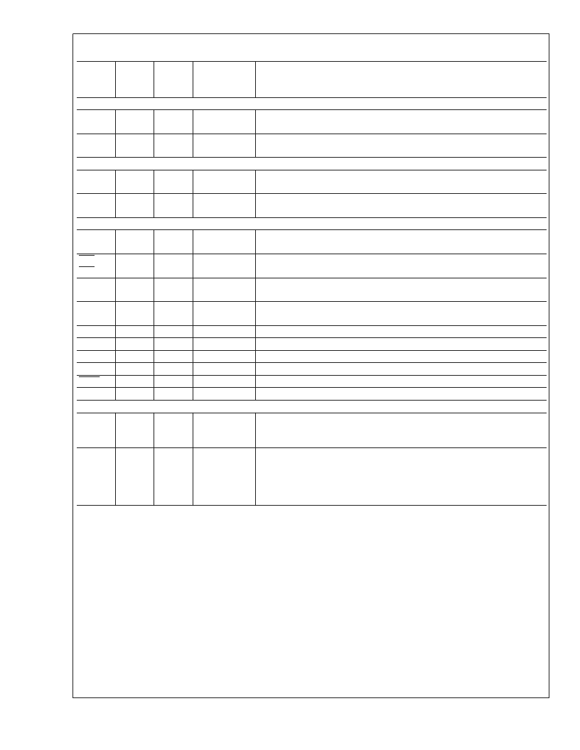
Pin Descriptions
Pin
Name
LLP Pin
Number
LQFP
Pin
Number
I/O, Type
Description
DIFFERENTIAL INPUTS COMMON TO ALL MUXES
IN0+
IN0
10
10
IN1+
IN1
13
14
SWITCHED DIFFERENTIAL OUTPUTS
OUT0+
OUT0
26
31
OUT1+
OUT1
23
27
DIGITAL CONTROL INTERFACE
SEL0,
SEL1
5
6
EN0,
EN1
15
17
PEM00,
PEM01
3
3
PEM10,
PEM11
1
1
TDI
19
22
TDO
20
23
TMS
18
21
TCK
17
19
TRST
21
24
N/C
8, 28
POWER
V
DD
11, 14,
16, 22,
25
29
GND
(Note 1)
5, 11, 15,
20, 26,
30
9
9
I, LVDS
Inverting and non-inverting differential inputs. LVDS, Bus LVDS, CML, or
LVPECL compatible.
Inverting and non-inverting differential inputs. LVDS, Bus LVDS, CML, or
LVPECL compatible.
12
13
I, LVDS
27
32
O, LVDS
Inverting and non-inverting differential outputs. OUT0
±
can be connected to any
one pair IN0
±
, or IN1
±
. LVDS compatible (Note 2).
Inverting and non-inverting differential outputs. OUT1
±
can be connected to any
one pair IN0
±
, or IN1
±
. LVDS compatible (Note 2).
24
28
O, LVDS
6
7
I, LVTTL
Select Control Inputs
7
8
I, LVTTL
Output Enable Inputs
4
4
I, LVTTL
Channel 0 Output Pre-emphasis Control Inputs
2
2
I, LVTTL
Channel 1 Output Pre-emphasis Control Inputs
I, LVTTL
O, LVTTL
I, LVTTL
I, LVTTL
I, LVTTL
Test Data Input to support IEEE 1149.1 features
Test Data Output to support IEEE 1149.1 features
Test Mode Select to support IEEE 1149.1 features
Test Clock to support IEEE 1149.1 features
Test Reset to support IEEE 1149.1 features
Not Connected
12, 16,
18, 25,
I, Power
V
DD
= 3.3V
±
0.3V. At least 4 low ESR 0.01 μF bypass capacitors should be
connected from V
DD
to GND plane.
Ground reference to LVDS and CMOS circuitry.
For the LLP package, the DAP is used as the primary GND connection to the
device. The DAP is the exposed metal contact at the bottom of the LLP-28
package. It should be connected to the ground plane with at least 4 vias for
optimal AC and thermal performance.
Note 1:
Note that for the LLP package GND is not an actual pin on the package, the GND is connected thru the DAP on the back side of the LLP package.
Note 2:
The LVDS outputs do not support a multidrop (BLVDS) environment. The LVDS output characteristics of the SCAN90CP02 device have been optimized for
point-to-point backplane and cable applications.
S
www.national.com
2
相關(guān)PDF資料 |
PDF描述 |
|---|---|
| SCAN90CP02SPX | 1.5 Gbps 2x2 LVDS Crosspoint Switch with Pre-Emphasis and IEEE 1149.6 |
| SCAN90CP02VY | Tape RoHS Compliant: Yes |
| SCAN921023SLC | 20-66 MHz 10 Bit Bus LVDS Serializer and Deserializer |
| SCAN921224 | 20-66 MHz 10 Bit Bus LVDS Serializer and Deserializer |
| SCAN921224SLC | 20-66 MHz 10 Bit Bus LVDS Serializer and Deserializer |
相關(guān)代理商/技術(shù)參數(shù) |
參數(shù)描述 |
|---|---|
| SCAN90CP02SP/NOPB | 功能描述:模擬和數(shù)字交叉點 IC RoHS:否 制造商:Micrel 配置:2 x 2 封裝 / 箱體:MLF-16 數(shù)據(jù)速率:10.7 Gbps 輸入電平:CML, LVDS, LVPECL 輸出電平:CML 電源電壓-最大:3.6 V 電源電壓-最小:2.375 V 最大工作溫度:+ 85 C 最小工作溫度:- 40 C 產(chǎn)品:Digital Crosspoint 封裝:Tube |
| SCAN90CP02SPX | 功能描述:模擬和數(shù)字交叉點 IC RoHS:否 制造商:Micrel 配置:2 x 2 封裝 / 箱體:MLF-16 數(shù)據(jù)速率:10.7 Gbps 輸入電平:CML, LVDS, LVPECL 輸出電平:CML 電源電壓-最大:3.6 V 電源電壓-最小:2.375 V 最大工作溫度:+ 85 C 最小工作溫度:- 40 C 產(chǎn)品:Digital Crosspoint 封裝:Tube |
| SCAN90CP02SPX/NOPB | 功能描述:模擬和數(shù)字交叉點 IC RoHS:否 制造商:Micrel 配置:2 x 2 封裝 / 箱體:MLF-16 數(shù)據(jù)速率:10.7 Gbps 輸入電平:CML, LVDS, LVPECL 輸出電平:CML 電源電壓-最大:3.6 V 電源電壓-最小:2.375 V 最大工作溫度:+ 85 C 最小工作溫度:- 40 C 產(chǎn)品:Digital Crosspoint 封裝:Tube |
| SCAN90CP02VY | 功能描述:模擬和數(shù)字交叉點 IC RoHS:否 制造商:Micrel 配置:2 x 2 封裝 / 箱體:MLF-16 數(shù)據(jù)速率:10.7 Gbps 輸入電平:CML, LVDS, LVPECL 輸出電平:CML 電源電壓-最大:3.6 V 電源電壓-最小:2.375 V 最大工作溫度:+ 85 C 最小工作溫度:- 40 C 產(chǎn)品:Digital Crosspoint 封裝:Tube |
| SCAN90CP02VY/NOPB | 功能描述:模擬和數(shù)字交叉點 IC RoHS:否 制造商:Micrel 配置:2 x 2 封裝 / 箱體:MLF-16 數(shù)據(jù)速率:10.7 Gbps 輸入電平:CML, LVDS, LVPECL 輸出電平:CML 電源電壓-最大:3.6 V 電源電壓-最小:2.375 V 最大工作溫度:+ 85 C 最小工作溫度:- 40 C 產(chǎn)品:Digital Crosspoint 封裝:Tube |
發(fā)布緊急采購,3分鐘左右您將得到回復。