- 您現(xiàn)在的位置:買賣IC網(wǎng) > PDF目錄374699 > SAF-C505L-4EM (INFINEON TECHNOLOGIES AG) 8-bit CMOS Microcontroller PDF資料下載
參數(shù)資料
| 型號: | SAF-C505L-4EM |
| 廠商: | INFINEON TECHNOLOGIES AG |
| 元件分類: | 8位微控制器 |
| 英文描述: | 8-bit CMOS Microcontroller |
| 中文描述: | 8位CMOS微控制器 |
| 文件頁數(shù): | 25/85頁 |
| 文件大?。?/td> | 487K |
| 代理商: | SAF-C505L-4EM |
第1頁第2頁第3頁第4頁第5頁第6頁第7頁第8頁第9頁第10頁第11頁第12頁第13頁第14頁第15頁第16頁第17頁第18頁第19頁第20頁第21頁第22頁第23頁第24頁當(dāng)前第25頁第26頁第27頁第28頁第29頁第30頁第31頁第32頁第33頁第34頁第35頁第36頁第37頁第38頁第39頁第40頁第41頁第42頁第43頁第44頁第45頁第46頁第47頁第48頁第49頁第50頁第51頁第52頁第53頁第54頁第55頁第56頁第57頁第58頁第59頁第60頁第61頁第62頁第63頁第64頁第65頁第66頁第67頁第68頁第69頁第70頁第71頁第72頁第73頁第74頁第75頁第76頁第77頁第78頁第79頁第80頁第81頁第82頁第83頁第84頁第85頁
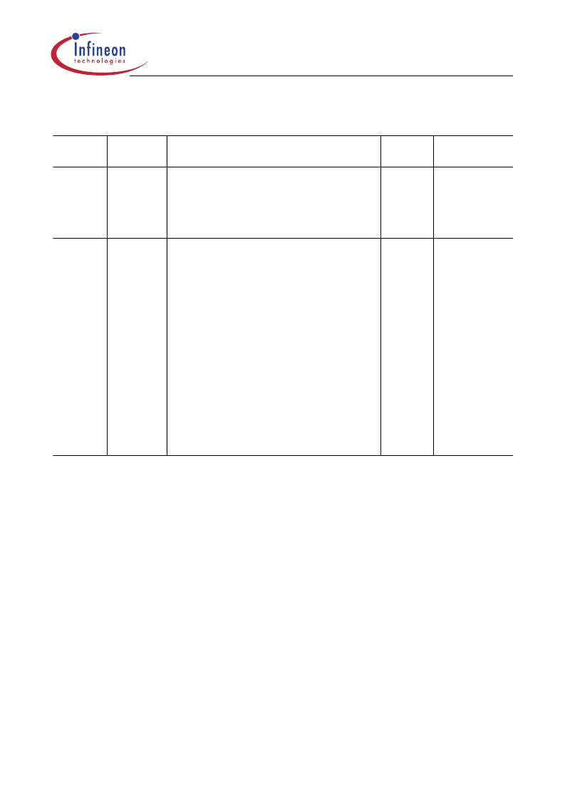
C505L
Data Sheet
23
06.99
LCD
Controller
DAC0
LCON
LCRL
LCRH
DIGn
5)
D/A Conversion Register
LCD Control Register
LCD Timer Reload Low Register
LCD Timer Reload High Register
LCD Digit Register ‘n’
5)
F3DC
H
F3DD
H
F3DE
H
F3DF
H
F3En
H
F3F0
H
F3F1
H
F3F2
H
F3F3
H
F3F4
H
F3F5
H
F3F6
H
F3F7
H
F3F8
H
F3F9
H
F3FA
H
F3FB
H
F3FC
H
F3FD
H
F3FE
H
F3FF
H
00
H
00
H
00
H
00
H
00
H
00
H
00
H
00
H
00
H
00
H
00
H
00
H
00
H
00
H
00
H
00
H
00
H
00
H
00
H
00
H
00
H
6)
6)
6)
6)
5) 6)
Real-Time
Clock
RTCON
RTCR0
RTCR1
RTCR2
RTCR3
RTCR4
CLREG0
CLREG1
CLREG2
CLREG3
CLREG4
RTINT0
RTINT1
RTINT2
RTINT3
RTINT4
Real-Time Clock Control Register
Real-Time Clock Initialization Register 0
Real-Time Clock Initialization Register 1
Real-Time Clock Initialization Register 2
Real-Time Clock Initialization Register 3
Real-Time Clock Initialization Register 4
Clock Count Register 0
Clock Count Register 1
Clock Count Register 2
Clock Count Register 3
Clock Count Register 4
Real-Time Clock Interrupt Register 0
Real-Time Clock Interrupt Register 1
Real-Time Clock Interrupt Register 2
Real-Time Clock Interrupt Register 3
Real-Time Clock Interrupt Register 4
6)
6)
6)
6)
6)
6)
6)
6)
6)
6)
6)
6)
6)
6)
6)
6)
1) Bit-addressable SFRs
2) This SFR is listed repeatedly since some bits of it also belong to other functional blocks.
3) “X” means that the value is undefined and the location is reserved.
4) SFR is located in the mapped SFR area. For accessing this SFR, bit RMAP in SFR SYSCON must be set.
5) The notation “n” (n = 0 to F) in the LCD Digit Register address definition defines the number of the related
LCD digit.
6) This register is located in the on-chip external data memory area.
Table 2
Special Function Registers - Functional Blocks
(cont’d)
Block
Symbol
Name
Address
Contents after
Reset
相關(guān)PDF資料 |
PDF描述 |
|---|---|
| SAB-C505 | 8-bit CMOS Microcontroller |
| SAF-C505L | 8-bit CMOS Microcontroller |
| SAB-C505L | 8-bit CMOS Microcontroller |
| SAF-C505 | 8-bit CMOS Microcontroller |
| SAFC505 | 8-bit CMOS Microcontroller |
相關(guān)代理商/技術(shù)參數(shù) |
參數(shù)描述 |
|---|---|
| SAF-C505-LM | 制造商:Rochester Electronics LLC 功能描述:- Bulk |
| SAFC5084EM | 制造商:Infineon Technologies AG 功能描述:MCU 8-bit C500 8051 CISC 32KB EPROM 5V 64-Pin MQFP |
| SAFC5084EMTR | 制造商:Infineon Technologies AG 功能描述:MCU 8-Bit C500 8051 CISC 32KB EPROM 5V 64-Pin MQFP T/R |
| SAFC5084EMTR-AA | 制造商:Infineon Technologies AG 功能描述:IC 8-BIT MCU |
| SAFC5084EMTR-AB | 制造商:Infineon Technologies AG 功能描述:IC,8-BIT MCU,0/70|C, P-MQFP-64 |
發(fā)布緊急采購,3分鐘左右您將得到回復(fù)。