- 您現在的位置:買賣IC網 > PDF目錄372108 > SAA1575HL (NXP SEMICONDUCTORS) Global Positioning System (GPS)baseband processor(通用定位系統(tǒng)基帶處理器) PDF資料下載
參數資料
| 型號: | SAA1575HL |
| 廠商: | NXP SEMICONDUCTORS |
| 元件分類: | 通信及網絡 |
| 英文描述: | Global Positioning System (GPS)baseband processor(通用定位系統(tǒng)基帶處理器) |
| 中文描述: | SPECIALTY TELECOM CIRCUIT, PQFP100 |
| 封裝: | 14 X 14 MM, 1.40 MM HEIGHT, PLASTIC, SOT-407-1, LQFP-100 |
| 文件頁數: | 9/56頁 |
| 文件大小: | 744K |
| 代理商: | SAA1575HL |
第1頁第2頁第3頁第4頁第5頁第6頁第7頁第8頁當前第9頁第10頁第11頁第12頁第13頁第14頁第15頁第16頁第17頁第18頁第19頁第20頁第21頁第22頁第23頁第24頁第25頁第26頁第27頁第28頁第29頁第30頁第31頁第32頁第33頁第34頁第35頁第36頁第37頁第38頁第39頁第40頁第41頁第42頁第43頁第44頁第45頁第46頁第47頁第48頁第49頁第50頁第51頁第52頁第53頁第54頁第55頁第56頁
1999 Jun 04
9
Philips Semiconductors
Product specification
Global Positioning System (GPS)
baseband processor
SAA1575HL
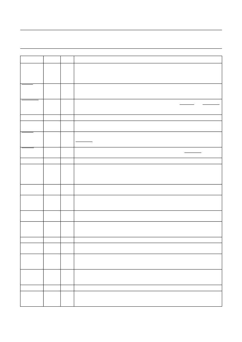
V
CC(R)
72
Backup core power supply
: 2.4 to 3.6 V only. Separate from the core supply to allow
a low capacity battery to be used to maintain the Real-Time Clock (RTC) function.
This should be powered from the main supply during normal operation and switched
to battery backup when the main supply fails.
External data memory select
: external RAM select pin, active LOW when the
external data memory space is addressed. This output is driven from V
CC(R)
and
V
CC(B)
supplies to ensure that the external RAM is not enabled during power-down.
Power fail indicator
: a LOW on this pin forces the embedded microcontroller into
reset. Reset will not be de-asserted until a set time after both PWRDN and PWRFAIL
go HIGH. For correct start-up, this pin should be LOW on power-up.
Crystal 4
: output from the RTC oscillator amplifier; this pin is only 3 V tolerant
Crystal 3
: input to inverting amplifier used in the RTC oscillator circuits (32.768 kHz);
this pin is only 3 V tolerant
Backup supply select
: this output is intended to drive an external FET used to switch
the battery backup supply(s). It is active LOW and is controlled directly by the
PWRFAIL.
Main supply select
: this output is intended to drive an external FET used to switch
the main supply(s). It is active LOW and is controlled directly by PWRFAIL.
Ground
: 0 V reference
Backup I/O power supply
: 2.4 to 5.5 V only. Supply for the RAM select, power fail
and power switching I/O pads only allowing these functions to be powered when the
main power supply fails. This should be powered from the main supply during normal
operation and switched to battery backup when the main supply fails.
Transmitter output 1
: transmit channel for serial port 1 (UART1) of the embedded
processor
Receiver input 1
: receive channel for serial port 1 (UART1) of the embedded
processor. It is intended that this serial port is dedicated to differential GPS
information (dependent on firmware).
Transmitter output 0
: transmit channel for serial port 0 (UART0) of the embedded
processor.
Receiver input 0
: receive channel for serial port 0 (UART0) of the embedded
processor. It is intended that this serial port is dedicated to the NMEA data stream
(dependent on firmware).
Ground
: 0 V reference
Main I/O power supply
: 2.7 to 5.5 V operating range; main supply for the periphery
in normal operation
GPIO bit 4
: standard general purpose I/O mapped into the segment 15 of the address
space. The top 4 bits can be used as the XA external timer control access pins
(T0, T1, T2 and T2EX).
GPIO bit 3
: standard general purpose I/O mapped into the segment 15 of the address
space. The top 4 bits can be used as the XA external timer control access pins
(T0, T1, T2 and T2EX).
RFIC set-up data
: serial data output used to set up the UAA1570HL front-end IC.
RFIC set-up data
: clock output for the serial data output used to set up the
UAA1570HL front-end IC. The state of the RFDAT and RFLE lines is latched into the
front-end IC on the rising edge.
DMCS
73
O
PWRFAIL
74
I
XTAL4
XTAL3
75
76
O
I
PWRB
77
O
PWRM
78
O
V
SS
V
CC(B)
79
80
TXD1
81
O
RXD1
82
I
TXD0
83
O
RXD0
84
I
V
SS
V
CC(P)
85
86
GPIO4
87
I/O
GPIO3
88
I/O
RFDAT
RFCLK
89
90
O
O
SYMBOL
PIN
I/O
DESCRIPTION
相關PDF資料 |
PDF描述 |
|---|---|
| SAA2023GP | Drive processor for DCC systems |
| SAA2023 | Drive processor for DCC systems |
| SAA2023H | RES 4.53K OHM 1/16W 0.5% 0402SMD |
| SAA2500 | MPEG Audio Source Decoder |
| SAA2500H | MPEG Audio Source Decoder |
相關代理商/技術參數 |
參數描述 |
|---|---|
| SAA158 | 制造商:SEMIKRON 制造商全稱:Semikron International 功能描述:Fast Avalanche Diodes |
| SAA159 | 制造商:SEMIKRON 制造商全稱:Semikron International 功能描述:Fast Avalanche Diodes |
| SAA160 | 制造商:SEMIKRON 制造商全稱:Semikron International 功能描述:Fast Avalanche Diodes |
| SAA16M8YX6XR4TL | 制造商:未知廠家 制造商全稱:未知廠家 功能描述:DOUBLE DATA RATE (DDR) SDRAM |
| SAA16M8YX6XV4TL | 制造商:未知廠家 制造商全稱:未知廠家 功能描述:DOUBLE DATA RATE (DDR) SDRAM |
發(fā)布緊急采購,3分鐘左右您將得到回復。