- 您現(xiàn)在的位置:買賣IC網(wǎng) > PDF目錄192306 > S71GL128NC0BAWAZ0 (SPANSION LLC) SPECIALTY MEMORY CIRCUIT, PBGA84 PDF資料下載
參數(shù)資料
| 型號: | S71GL128NC0BAWAZ0 |
| 廠商: | SPANSION LLC |
| 元件分類: | 存儲器 |
| 英文描述: | SPECIALTY MEMORY CIRCUIT, PBGA84 |
| 封裝: | 8 X 11.60 MM, 1.20 MM HEIGHT, LEAD FREE COMPLIANT, FBGA-84 |
| 文件頁數(shù): | 92/122頁 |
| 文件大小: | 1764K |
| 代理商: | S71GL128NC0BAWAZ0 |
第1頁第2頁第3頁第4頁第5頁第6頁第7頁第8頁第9頁第10頁第11頁第12頁第13頁第14頁第15頁第16頁第17頁第18頁第19頁第20頁第21頁第22頁第23頁第24頁第25頁第26頁第27頁第28頁第29頁第30頁第31頁第32頁第33頁第34頁第35頁第36頁第37頁第38頁第39頁第40頁第41頁第42頁第43頁第44頁第45頁第46頁第47頁第48頁第49頁第50頁第51頁第52頁第53頁第54頁第55頁第56頁第57頁第58頁第59頁第60頁第61頁第62頁第63頁第64頁第65頁第66頁第67頁第68頁第69頁第70頁第71頁第72頁第73頁第74頁第75頁第76頁第77頁第78頁第79頁第80頁第81頁第82頁第83頁第84頁第85頁第86頁第87頁第88頁第89頁第90頁第91頁當(dāng)前第92頁第93頁第94頁第95頁第96頁第97頁第98頁第99頁第100頁第101頁第102頁第103頁第104頁第105頁第106頁第107頁第108頁第109頁第110頁第111頁第112頁第113頁第114頁第115頁第116頁第117頁第118頁第119頁第120頁第121頁第122頁
December 15, 2004 S29GLxxxN_MCP_A1
S29GLxxxN MirrorBitTM Flash Family
71
Ad vance
Info rmat i o n
be at VHH for operations other than accelerated programming, or device damage
may result. WP# has an internal pullup; when unconnected, WP# is at VIH.
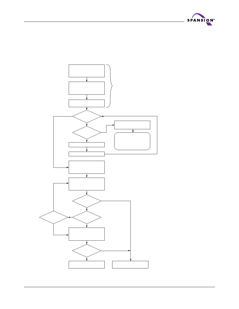
Figure 2 illustrates the algorithm for the program operation. Refer to the Erase
and Program Operations–“AC Characteristics” section for parameters, and Figure
14 for timing diagrams.
Figure 1. Write Buffer Programming Operation
Write “Write to Buffer”
command and
Sector Address
Write number of addresses
to program minus 1(WC = 31)
and Sector Address
Write program buffer to
flash sector address
Write first address/data
Write to a different
sector address
FAIL or ABORT
PASS
Read DQ15 - DQ0 at
Last Loaded Address
Read DQ15 - DQ0 with
address = Last Loaded
Address
Write next address/data pair
WC = WC - 1
WC = 0 ?
Part of “Write to Buffer”
Command Sequence
Yes
No
Abort Write to
Buffer Operation?
DQ7 = Data?
DQ5 = 1?
DQ1 = 1?
Write to buffer ABORTED.
Must write “Write-to-buffer
Abort Reset” command
sequence to return
to read mode.
Notes:
1. When Sector Address is specified, any
address in the selected sector is acceptable.
However, when loading Write-Buffer
address locations with data, all addresses
must fall within the selected Write-Buffer
Page.
2. DQ7 may change simultaneously with DQ5.
Therefore, DQ7 should be verified.
3. If this flowchart location was reached
because DQ5= “1”, then the device FAILED.
If this flowchart location was reached
because DQ1= “1”, then the Write to Buffer
operation was ABORTED. In either case, the
proper reset command must be written
before the device can begin another
operation. If DQ1=1, write the Write-
Buffer-Programming-Abort-Reset
command. if DQ5=1, write the Reset
command.
4. See Table 12 for command sequences
required for write buffer programming.
相關(guān)PDF資料 |
PDF描述 |
|---|---|
| S71PL064JB0BFW0U0 | SPECIALTY MEMORY CIRCUIT, PBGA56 |
| S71PL129JC0BFW9Z2 | Stacked Multi-Chip Product (MCP) Flash Memory |
| S71PL129NC0HFW4U3 | SPECIALTY MEMORY CIRCUIT, PBGA64 |
| S71PL191HB0BFI100 | SPECIALTY MEMORY CIRCUIT, PBGA73 |
| S71VS128RC0ZHK203 | SPECIALTY MEMORY CIRCUIT, PBGA56 |
相關(guān)代理商/技術(shù)參數(shù) |
參數(shù)描述 |
|---|---|
| S71GL256NB0 | 制造商:SPANSION 制造商全稱:SPANSION 功能描述:Stacked Multi-chip Product (MCP) |
| S71GL256NC0 | 制造商:SPANSION 制造商全稱:SPANSION 功能描述:Stacked Multi-chip Product (MCP) |
| S71GL512NB0 | 制造商:SPANSION 制造商全稱:SPANSION 功能描述:Stacked Multi-chip Product (MCP) |
| S71GL512NC0 | 制造商:SPANSION 制造商全稱:SPANSION 功能描述:Stacked Multi-chip Product (MCP) |
| S71GL-N | 制造商:SPANSION 制造商全稱:SPANSION 功能描述:Stacked Multi-Chip Product (MCP) Flash Memory and RAM |
發(fā)布緊急采購,3分鐘左右您將得到回復(fù)。