- 您現(xiàn)在的位置:買賣IC網(wǎng) > PDF目錄368610 > S1L9226X (SAMSUNG SEMICONDUCTOR CO. LTD.) RF AMP & SERVO SIGNAL PROCESSOR PDF資料下載
參數(shù)資料
| 型號: | S1L9226X |
| 廠商: | SAMSUNG SEMICONDUCTOR CO. LTD. |
| 英文描述: | RF AMP & SERVO SIGNAL PROCESSOR |
| 中文描述: | 射頻放大器 |
| 文件頁數(shù): | 47/56頁 |
| 文件大小: | 454K |
| 代理商: | S1L9226X |
第1頁第2頁第3頁第4頁第5頁第6頁第7頁第8頁第9頁第10頁第11頁第12頁第13頁第14頁第15頁第16頁第17頁第18頁第19頁第20頁第21頁第22頁第23頁第24頁第25頁第26頁第27頁第28頁第29頁第30頁第31頁第32頁第33頁第34頁第35頁第36頁第37頁第38頁第39頁第40頁第41頁第42頁第43頁第44頁第45頁第46頁當(dāng)前第47頁第48頁第49頁第50頁第51頁第52頁第53頁第54頁第55頁第56頁
RF AMP & SERVO SIGNAL PROCESSOR
S1L9226X
5
PRELIMINARY
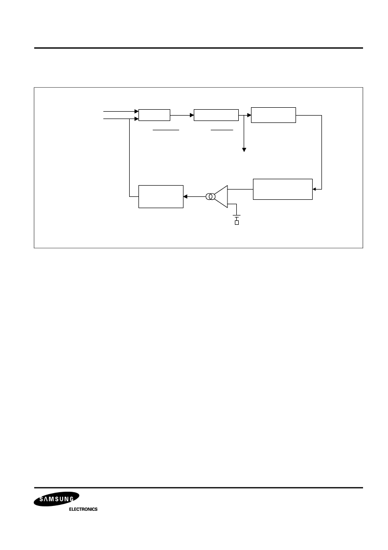
RF EQUALIZE & AGC
The modulator output, which had the Veqc's Tanh term multiplied at the input, passes through the approximately
3X gain terminal to the ARF pad. On the one hand, the output is - rectified as it passes through the HPF having
50kHz pole frequency and follows the peak envelope the RF level. At this time, the pole frequency of the HPF is
set to 50kHz so that the 3T - 11T component can pass through without attenuation. The RF level peak value is
integrated at the 's CAP node after wave rectification. If this peak value is less than the already set voltage
comparison, sinking current is output and, if not, sourcing current is output. The maximum peak value at this time is
10uA, which is I/V converted and applied as the modulator control voltage. Under the sinking condition, the Vcagc
increases to 1outx10K and multiplied by Tanh (1-X); the sourcing condition, Vcagc decreases to Iout x10K and
multiplied by Tanh (1+X), where X is (Veqc/2Vt).
Overall, after detecting the 3T and 11T levels by full-wave rectification, it is compared to Tanh using the modulator
and multiplied to the gain to realize the wave-form equalize. The above is related to the AGC concept, which
means that a specific RF level is always taken
Modulator
3x Gain AMP
HPF
(3dB: 50kHz)
I/V Converter
Control Range
I * 10K
Full Wave Rectifier
(RF Peak Envelope)
Iout = 2gm (Vid/2)
= gm * Vid
= (Iref) * (Vid/Vt)
= Iref * (Vp-Vn)/Vt
if Vn > Vp
Vcagc Increment (tanh (1-X))
if Vn < Vp
Vcagc Decrement (tanh (1+X))
tanh
±
0.1 =
±
0.1
tanh
±
0.5 =
±
0.462
tanh
±
0.1 =
±
0.7
tanh
±
2.0 =
±
0.964
Vref
Vp
Vn
V = I/C (115pF)
EQO-AGC Output
Vin (t)
Vcagc (t)
Vo (t)
+
-
Vin(t) = 0.73x (RFO)
Vo(t) =
R6 (5.5K)
(
2Vt
Vcagc(t)
)
相關(guān)PDF資料 |
PDF描述 |
|---|---|
| S1L9226X01-Q0R0 | RF AMP & SERVO SIGNAL PROCESSOR |
| S1L9251X | CD-ROM 48X RF AMP |
| S1M8662A | CDMA/PCS/GPS Triple Mode IF/ baseband IC |
| S1M8662AX01-F0T0 | CDMA/PCS/GPS Triple Mode IF/ baseband IC |
| S1M8836 | FRACTIONAL-N RF/INTEGER-N IF DUAL PLL |
相關(guān)代理商/技術(shù)參數(shù) |
參數(shù)描述 |
|---|---|
| S1L9226X01 | 制造商:SAMSUNG 制造商全稱:Samsung semiconductor 功能描述:RF AMP & SERVO SIGNAL PROCESSOR |
| S1L9226X01-Q0R0 | 制造商:SAMSUNG 制造商全稱:Samsung semiconductor 功能描述:RF AMP & SERVO SIGNAL PROCESSOR |
| S1L9251X | 制造商:SAMSUNG 制造商全稱:Samsung semiconductor 功能描述:CD-ROM 48X RF AMP |
| S1LB_FDSS517 WAF | 制造商:Fairchild Semiconductor Corporation 功能描述: |
| S1LL | 制造商:HY 制造商全稱:HY ELECTRONIC CORP. 功能描述:SURFACE MOUNT GLASS PASSIVATED RECTIFIERS |
發(fā)布緊急采購,3分鐘左右您將得到回復(fù)。