- 您現(xiàn)在的位置:買賣IC網(wǎng) > PDF目錄376330 > S12MSCANV2D (Motorola, Inc.) MC9S12DT128 Device User Guide V02.09 PDF資料下載
參數(shù)資料
| 型號: | S12MSCANV2D |
| 廠商: | Motorola, Inc. |
| 英文描述: | MC9S12DT128 Device User Guide V02.09 |
| 中文描述: | MC9S12DT128設(shè)備的用戶手冊V02.09 |
| 文件頁數(shù): | 89/138頁 |
| 文件大小: | 2083K |
| 代理商: | S12MSCANV2D |
第1頁第2頁第3頁第4頁第5頁第6頁第7頁第8頁第9頁第10頁第11頁第12頁第13頁第14頁第15頁第16頁第17頁第18頁第19頁第20頁第21頁第22頁第23頁第24頁第25頁第26頁第27頁第28頁第29頁第30頁第31頁第32頁第33頁第34頁第35頁第36頁第37頁第38頁第39頁第40頁第41頁第42頁第43頁第44頁第45頁第46頁第47頁第48頁第49頁第50頁第51頁第52頁第53頁第54頁第55頁第56頁第57頁第58頁第59頁第60頁第61頁第62頁第63頁第64頁第65頁第66頁第67頁第68頁第69頁第70頁第71頁第72頁第73頁第74頁第75頁第76頁第77頁第78頁第79頁第80頁第81頁第82頁第83頁第84頁第85頁第86頁第87頁第88頁當(dāng)前第89頁第90頁第91頁第92頁第93頁第94頁第95頁第96頁第97頁第98頁第99頁第100頁第101頁第102頁第103頁第104頁第105頁第106頁第107頁第108頁第109頁第110頁第111頁第112頁第113頁第114頁第115頁第116頁第117頁第118頁第119頁第120頁第121頁第122頁第123頁第124頁第125頁第126頁第127頁第128頁第129頁第130頁第131頁第132頁第133頁第134頁第135頁第136頁第137頁第138頁
MC9S12DT128 Device User Guide — V02.09
89
Section 21 Port Integration Module (PIM) Block Description
Consult the PIM_9DTB128 Block User Guide for information about the Port Integration Module.
Section 22 Voltage Regulator (VREG) Block Description
Consult the VREG Block User Guide for information about the dual output linear voltage regulator.
Section 23 Printed Circuit Board Layout Proposal
The PCB must be carefully laid out to ensure proper operation of the voltage regulator as well as of the
MCU itself. The following rules must be observed:
Every supply pair must be decoupled by a ceramic capacitor connected as near as possible to the
corresponding pins (C1 –C6).
Central point of the ground star should be the VSSR pin.
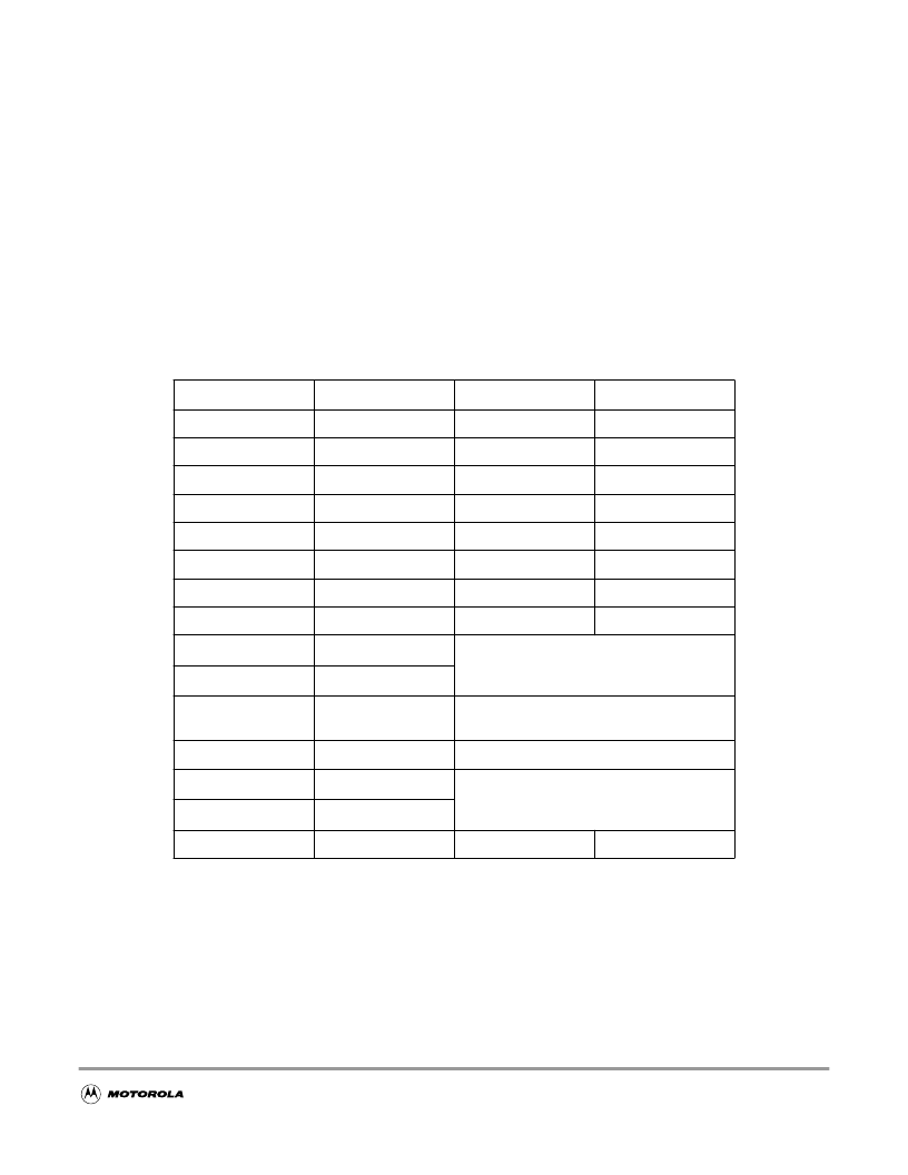
Table 23-1 Suggested External Component Values
Component
Purpose
Type
Value
C1
VDD1 filter cap
ceramic X7R
100 … 220nF
C2
VDD2 filter cap
ceramic X7R
100 … 220nF
C3
VDDA filter cap
ceramic X7R
100nF
C4
VDDR filter cap
X7R/tantalum
>= 100nF
C5
VDDPLL filter cap
ceramic X7R
100nF
C6
VDDX filter cap
X7R/tantalum
>= 100nF
C7
OSC load cap
C8
OSC load cap
C9 / C
S
PLL loop filter cap
See PLL specification chapter
C10 / C
P
PLL loop filter cap
C11 / C
DC
DC cutoff cap
Colpitts mode only, if recommended by
quartz manufacturer
R1 / R
PLL loop filter res
See PLL Specification chapter
R2 / R
B
Pierce mode only
R3 / R
S
Q1
Quartz
相關(guān)PDF資料 |
PDF描述 |
|---|---|
| S20100 | Silicon Power Rectifier |
| S20120 | Silicon Power Rectifier |
| S2020 | Silicon Power Rectifier |
| S2040 | Silicon Power Rectifier |
| S204 | Silicon Power Rectifier |
相關(guān)代理商/技術(shù)參數(shù) |
參數(shù)描述 |
|---|---|
| S12N11F-A | 制造商:TE Connectivity 功能描述: |
| S12N2.5A-G | 制造商:TE Connectivity 功能描述: |
| S12N2A-G1 | 制造商:TE Connectivity 功能描述: |
| S12N3W3C | 制造商:HB 制造商全稱:HB Electronic Components 功能描述:LED |
| S12N3W6C | 制造商:HB 制造商全稱:HB Electronic Components 功能描述:LED |
發(fā)布緊急采購,3分鐘左右您將得到回復(fù)。