- 您現在的位置:買賣IC網 > PDF目錄225135 > S-8232AYFT-T2 2-CHANNEL POWER SUPPLY SUPPORT CKT, PDSO8 PDF資料下載
參數資料
| 型號: | S-8232AYFT-T2 |
| 元件分類: | 電源管理 |
| 英文描述: | 2-CHANNEL POWER SUPPLY SUPPORT CKT, PDSO8 |
| 封裝: | TSSOP-8 |
| 文件頁數: | 24/26頁 |
| 文件大?。?/td> | 729K |
| 代理商: | S-8232AYFT-T2 |
BATTERY PROTECTION IC FOR 2-CELL SERIAL PACK
Rev.4.3_01
S-8232 Series
Seiko Instruments Inc.
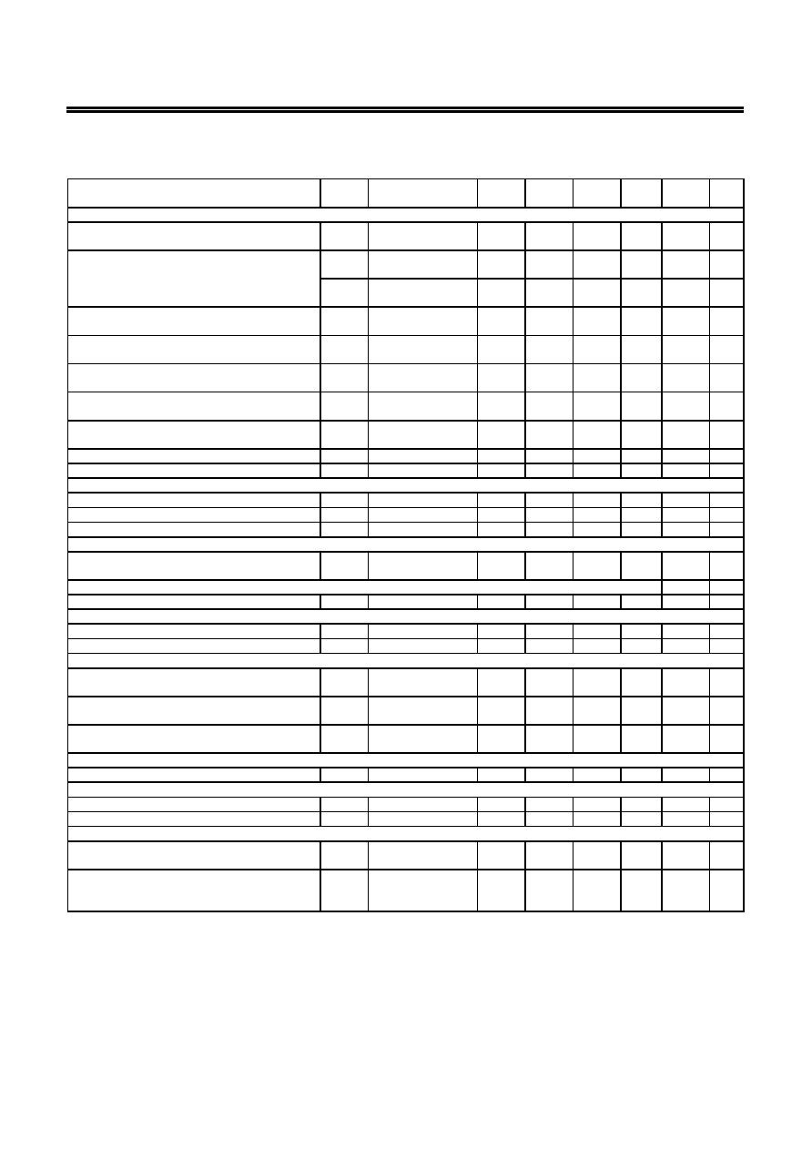
7
Table 6
(Ta
= 20 to + 70 °C unless otherwise specified)
Item
Symbol
Condition
Min.
Typ.
Max.
Unit
Test
Condition
Test
Circuit
[DETECTION VOLTAGE]
Overcharge detection voltage 1, 2
VCU1,2 3.90 to 4.60 V,
Adjustable
VCU1,2
0.045
VCU1,2
+ 0.040
V
1, 2
1
VCUaux1,2 VCU1,2
× 1.25
VCU1,2
× 1.19
VCU1,2
× 1.25
VCU1,2
× 1.31
V
1, 2
1
Auxiliary overcharge detection voltage 1, 2
*1
VCUaux1, VCUaux2
= VCU1, VCU2 × 1.25 or
VCUaux1, VCUaux2
= VCU1, VCU2 × 1.11
VCUaux1,2 VCU1,2
× 1.11
VCU1,2
× 1.05
VCU1,2
× 1.11
VCU1,2
× 1.17
V
1, 2
1
Overcharge release voltage 1, 2
VCD1,2 3.60 to 4.60 V,
Adjustable
VCD1,2
0.070
VCD1,2
+ 0.065
V
1, 2
1
Overdischarge detection voltage 1, 2
VDD1,2 1.70 to 2.60 V,
Adjustable
VDD1,2
0.100
VDD1,2
+ 0.095
V
1, 2
1
Overdischarge release voltage 1, 2
VDU1,2 1.70 to 3.80 V,
Adjustable
VDU1,2
0.120
VDU1,2
+ 0.115
V
1, 2
1
Overcurrent detection voltage 1
VIOV1 0.07 to 0.30 V,
Adjustable
VIOV1
0.029
VIOV1
+ 0.029
V
3
1
Overcurrent detection voltage 2
VIOV2 Load short circuit,
VCC reference
1.66 1.20 0.74
V
3
1
Temperature coefficient 1 for detection voltage *2
TCOE1 Ta
= 40 to + 85 °C 0.6
0
0.6
mV/°C
Temperature coefficient 2 for detection voltage *3
TCOE2 Ta
= 40 to + 85 °C 0.24 0.05
0
mV/°C
[DELAY TIME (C3
= 0.22 F) ]
Overcharge detection delay time 1, 2
tCU1,2 1.0 s
0.60
1.00
1.84
s
8, 9
5
Overdischarge detection delay time 1, 2
tDD1,2 0.1 s
67
100
140
ms
8, 9
5
Overcurrent detection delay time 1
tIOV1 0.01 s
6.5
10
14.5
ms
10
5
[INPUT VOLTAGE]
Input voltage between VCC and VSS
VDS
Absolute maximum
rating
0.3
18
V
[OPERATING VOLTAGE]
Operating voltage between VCC and VSS *4
VDSOP Output logic fixed
2.0
16
V
[CURRENT CONSUMPTION]
Current consumption during normal operation
IOPE V1
= V2 = 3.6 V
1.9
7.5
13.8
A
4
2
Current consumption at power down
IPDN V1
= V2 = 1.5 V
0
0.0002
0.06
A
4
2
[OUTPUT VOLTAGE]
DO voltage “H”
VDOH IOUT
= 10 A
VCC
0.14
VCC
0.003
VCC
V
6
3
DO voltage “L”
VDOL IOUT
= 10 A
VSS
+ 0.003
VSS
+ 0.14
V
6
3
CO voltage “H”
VCOH IOUT
= 10 A
VCC
0.24
VCC
0.019
VCC
V
7
4
[CO PIN INTERNAL RESISTANCE]
Resistance between VSS and CO
RCOL VCO
VSS = 9.4 V
0.24
0.6
1.96
M
7
4
[INTERNAL RESISTANCE]
Resistance between VCC and VM
Rvcm VCC
VVM = 0.5 V
86
240
785
k
5
2
Resistance between VSS and VM
Rvsm VVM
VSS= 1.1 V
418
597
1332
k
5
2
[0 V BATTERY CHARGE FUNCTION]
0 V battery charge starting charger voltage
V0CHA 0 V battery charging
function “available”
0.29
0.75
1.21
V
11
6
0 V battery charge inhibition battery voltage 1, 2
V0INH1,2
0 V battery charging
function
“unavailable”
0.23
0.88
1.53
V
12, 13
6
*1. Auxiliary overcharge detection voltage is equal to the overcharge detection voltage times 1.11 for the
products without overcharge hysteresis, and times 1.25 for other products.
*2. Temperature coefficient 1 for detection voltage should be applied to overcharge detection voltage,
overcharge release voltage, overdischarge detection voltage, and overdischarge release voltage.
*3. Temperature coefficient 2 for detection voltage should be applied to overcurrent detection voltage.
*4. The DO pin and CO pin logic are established at the operating voltage.
相關PDF資料 |
PDF描述 |
|---|---|
| S-8233CAFT | 3-CHANNEL POWER SUPPLY SUPPORT CKT, PDSO16 |
| S-8241ABXMC-GBX-T2 | 1-CHANNEL POWER SUPPLY SUPPORT CKT, PDSO5 |
| S-8241ABZPN-KBZ-TFG | 1-CHANNEL POWER SUPPLY SUPPORT CKT, PDSO5 |
| S-8241ACJPN-KCJ-TFG | 1-CHANNEL POWER SUPPLY SUPPORT CKT, PDSO5 |
| S-8261ACAMD-G4AT2G | 1-CHANNEL POWER SUPPLY SUPPORT CKT, PDSO6 |
相關代理商/技術參數 |
參數描述 |
|---|---|
| S-8232AYFT-T2-G | 功能描述:電池管理 Lithium-Ion battery protection (2 cell) RoHS:否 制造商:Texas Instruments 電池類型:Li-Ion 輸出電壓:5 V 輸出電流:4.5 A 工作電源電壓:3.9 V to 17 V 最大工作溫度:+ 85 C 最小工作溫度:- 40 C 封裝 / 箱體:VQFN-24 封裝:Reel |
| S-8232AZFT-T2-G | 功能描述:電池管理 Lithium-Ion battery protection (2 cell) RoHS:否 制造商:Texas Instruments 電池類型:Li-Ion 輸出電壓:5 V 輸出電流:4.5 A 工作電源電壓:3.9 V to 17 V 最大工作溫度:+ 85 C 最小工作溫度:- 40 C 封裝 / 箱體:VQFN-24 封裝:Reel |
| S8232GM4NR | 制造商:TYAN 功能描述:(2)SR5690, G34, (12+12) DDR3 DIMMS - Bulk |
| S-8232NAFT-T2-G | 功能描述:電池管理 Lithium-Ion battery protection (2 cell) RoHS:否 制造商:Texas Instruments 電池類型:Li-Ion 輸出電壓:5 V 輸出電流:4.5 A 工作電源電壓:3.9 V to 17 V 最大工作溫度:+ 85 C 最小工作溫度:- 40 C 封裝 / 箱體:VQFN-24 封裝:Reel |
| S-8232NBFT-T2-G | 制造商:SII 制造商全稱:Seiko Instruments Inc 功能描述:BATTERY PROTECTION IC FOR 2-SERIAL-CELL PACK |
發(fā)布緊急采購,3分鐘左右您將得到回復。