- 您現(xiàn)在的位置:買賣IC網(wǎng) > PDF目錄373328 > RT9241B PDF資料下載
參數(shù)資料
| 型號: | RT9241B |
| 文件頁數(shù): | 11/18頁 |
| 文件大小: | 333K |
| 代理商: | RT9241B |
RT9241A/B
DS9241AB-01 October 2002
www.richtek.com
11
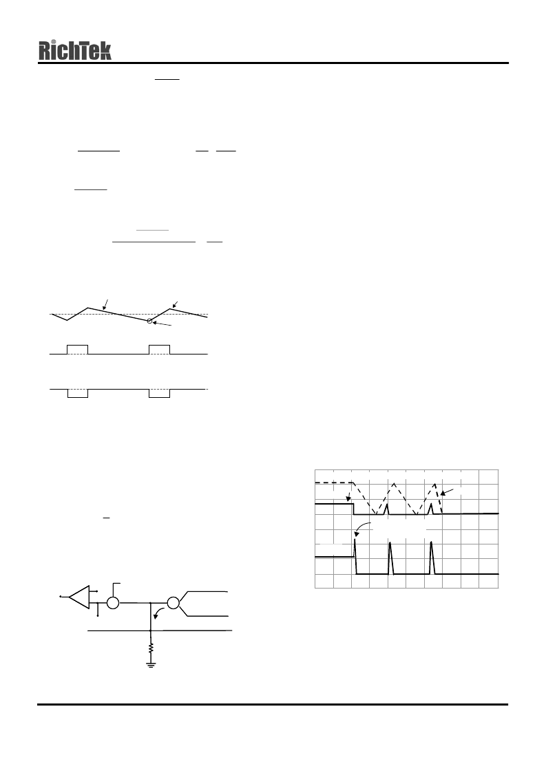
The sensing circuit gets I
X
= by local
feedback. R
SP
= R
SN
to cancel the voltage drop
caused by GM amplifier input bias current. I
X
is
sampled and held just before low side MOSFET turns
off (See Fig.2). Therefore, trip point of OVP is 120% of normal output level. The
,
,
T
S
, for switching
period = T
S
Soft start circuit generates a ramp voltage by charging
external capacitor with 10uA current after IC POR
acts. The PWM pulse width and V
CORE
are clamped
by the rising ramp to reduce the in-rush current and
protect the power components.
I
L (S/H)
Inductor Current
Fig. 2 Inductor Current and PWM Signal
Droop tuning
The S/H current signals from power channels are
injected to ADJ pin to create droop voltage.
The DAC output voltage decreases by V
ADJ
to form
the VCORE load droop(see Fig.3).
Protection and SS function
For OVP, the RT9241A/B detects the V
CORE
by V
SEN
pin. Eliminate the parasitic delay and noise influence
on the PCB path for fast and accurate detection. The
PWM outputs are pulled low to turn on the low side
MOSFET and turn off the high side MOSFET of the
synchronous rectifier at OVP. The OVP latch can only
be reset by V
DD
or V
DVD
restart power on reset
sequence. The PGOOD detection trip point of V
CORE
is
±
8% out of the normal level. The PGOOD open
drain output pulls low when V
OCRE
exceeds the
range.
OCP is triggered if one channel S/H current signal I
X
>
75
μ
A. Controller forces PWM output latched at high
impedance to turn off both high and low side
MOSFET in the power stage and initial the hiccup
mode protection. The SS pin voltage is pulled low with
a 10
μ
A current after it is less than 90% V
DD
. The
converter restarts after SS pin voltage < 0.2V. Three
times of OCP disable the converter and only release
the latch by POR acts (see Fig.4).
Fig. 4
Fig. 3 Droop Tune Circuit
L
R
I
S
)
H
/
S
(
2
OFF
O
V
IN
∑
×
=
X
ADJ
ADJ
I
3
2
R
V
0A
0V
2V
4V
T0T1
T2
T3T4
TIME
COUNT = 1
COUNT = 2
COUNT = 3
OVERLOAD
APPLIED
SS
V
CORE
I
L
Falling Slope = V
O
/L
I
L
I
L (AVG)
PWM Signal & High Side MOSFET Gate Signal
Low Side MOSFET Gate Signal
SP
S
IN
L
2
O
IN
V
O
)
AVG
(
L
I
)
H
/
S
(
X
I
R
R
T
S
V
V
V
×
×
=
+
_
EA
∑
FB
COMP
V
DAC
- V
ADJ
+
_
V
DAC
V
ADJ
ADJ
R
ADJ
2/3 I
X1
2/3 I
X2
∑
I
X
相關(guān)PDF資料 |
PDF描述 |
|---|---|
| RT9241A | |
| RT9261 | Step-up DC/DC Converter |
| RT9261A | Step-up DC/DC Converter |
| RT9266 | Step-up DC/DC Converter |
| RT9266B | Step-up DC/DC Converter |
相關(guān)代理商/技術(shù)參數(shù) |
參數(shù)描述 |
|---|---|
| RT9241BGS | 制造商:RICHTEK 制造商全稱:Richtek Technology Corporation 功能描述:Two-Phase DC/DC Controller for CPU Core Power Supply |
| RT9241BPS | 制造商:RICHTEK 制造商全稱:Richtek Technology Corporation 功能描述:Two-Phase DC/DC Controller for CPU Core Power Supply |
| RT9241CS | 制造商:未知廠家 制造商全稱:未知廠家 功能描述:Two-Phase DC/DC Controller for CPU Core Power Supply |
| RT9243 | 制造商:RICHTEK 制造商全稱:Richtek Technology Corporation 功能描述:Multi-Phase PWM Controller for CPU Core Power Supply |
| RT9243GS | 制造商:RICHTEK 制造商全稱:Richtek Technology Corporation 功能描述:Multi-Phase PWM Controller for CPU Core Power Supply |
發(fā)布緊急采購,3分鐘左右您將得到回復(fù)。