- 您現(xiàn)在的位置:買賣IC網(wǎng) > PDF目錄373328 > RT9237A PDF資料下載
參數(shù)資料
| 型號: | RT9237A |
| 文件頁數(shù): | 4/10頁 |
| 文件大小: | 163K |
| 代理商: | RT9237A |
RT9231A
www.richtek.com
4
DS9231A-02 July 2001
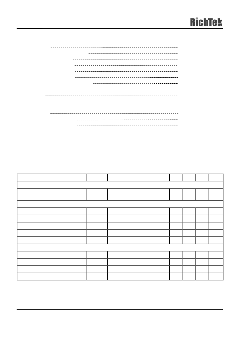
Absolute Maximum Ratings
z
Supply Voltage
z
PGOOD, FAULT and GATE Voltage
z
Input, Output or I/O Voltage
z
Ambient Temperature Range
z
Junction Temperature Range
z
Storage Temperature Range
z
Lead Temperature (Soldering, 10 sec.)
z
Package Thermal Resistance
SOP-28,
θ
JA
+15V
GND
0.3V ~ V
CC
+0.3V
GND
0.3V ~ 7V
0
°
C ~ +70
°
C
0
°
C ~ +125
°
C
65
°
C ~ +150
°
C
300
°
C
60
°
C/W
Recommended Operating Conditions
z
Supply Voltage
z
Ambient Temperature Range
z
Junction Temperature Range
+12V
±
10%
0
°
C to 70
°
C
0
°
C to 125
°
C
CAUTION:
Stresses beyond the ratings specified in “Absolute Maximum Ratings” may cause permanent damage to the
device. This is a stress only rating and operation of the device at these or any other conditions above those
indicated in the operational sections of this specification is not implied.
Electrical Characteristics
(V
CC
= 12V, PGND = 0V, T
A
= 25
°
C, Unless otherwise specified.)
Parameter
Symbol
Test Conditions
Min
Typ
Max
Units
VCC Supply Current
Nominal Supply Current
I
CC
UGATE, LGATE, DRIVE2,
DRIVE3, and DRIVE4 Open
--
10
--
mA
Power-On Reset
VCC Rising Threshold
V
OCSET
= 4.5V
7.5
--
9.5
V
VCC Falling Threshold
V
OCSET
= 4.5V
7
--
9
V
Rising VAUX Threshold
V
OCSET
= 4.5V
--
2.8
--
V
VAUX Threshold Hysteresys
V
OCSET
= 4.5V
--
0.5
--
V
Rising V
OCSET
Threshold
DAC and Band Gap Reference
--
1.25
--
V
DAC (VID0-VID4) Input Low Voltage
--
--
0.8
V
DAC (VID0-VID4) Input High Voltage
2.0
--
--
V
DACOUT Voltage Accuracy
-1
--
1
%
Band Gap Reference Voltage
V
BG
1.240 1.265 1.290
V
To be continued
相關(guān)PDF資料 |
PDF描述 |
|---|---|
| RT9241B | |
| RT9241A | |
| RT9261 | Step-up DC/DC Converter |
| RT9261A | Step-up DC/DC Converter |
| RT9266 | Step-up DC/DC Converter |
相關(guān)代理商/技術(shù)參數(shù) |
參數(shù)描述 |
|---|---|
| RT9237CS | 制造商:未知廠家 制造商全稱:未知廠家 功能描述:MULTI-PHASE DC/DC CONTROLLER FOR CPU CORE POWER SUPPLY |
| RT9238 | 制造商:未知廠家 制造商全稱:未知廠家 功能描述:VRM 8.5 PWM AND TRIPLE LINEAR POWER SYSTEM CONTROLLER |
| RT9238CS | 制造商:未知廠家 制造商全稱:未知廠家 功能描述:VRM 8.5 PWM AND TRIPLE LINEAR POWER SYSTEM CONTROLLER |
| RT9241 | 制造商:未知廠家 制造商全稱:未知廠家 功能描述:Two-Phase DC/DC Controller for CPU Core Power Supply |
| RT9241A | 制造商:未知廠家 制造商全稱:未知廠家 功能描述: |
發(fā)布緊急采購,3分鐘左右您將得到回復(fù)。