- 您現(xiàn)在的位置:買賣IC網(wǎng) > PDF目錄373293 > RM3183CH Line Receiver PDF資料下載
參數(shù)資料
| 型號: | RM3183CH |
| 元件分類: | 接收器 |
| 英文描述: | Line Receiver |
| 中文描述: | 線路接收器 |
| 文件頁數(shù): | 10/45頁 |
| 文件大小: | 287K |
| 代理商: | RM3183CH |
第1頁第2頁第3頁第4頁第5頁第6頁第7頁第8頁第9頁當(dāng)前第10頁第11頁第12頁第13頁第14頁第15頁第16頁第17頁第18頁第19頁第20頁第21頁第22頁第23頁第24頁第25頁第26頁第27頁第28頁第29頁第30頁第31頁第32頁第33頁第34頁第35頁第36頁第37頁第38頁第39頁第40頁第41頁第42頁第43頁第44頁第45頁
www.fairchildsemi.com
Features
Adjustable rise and fall times
Low supply current
Capable of driving 30 nF || 400
Digitally selectable 12.5 or 100 kbit/sec data rate
Adjustable output voltages swing
Output overvoltage protected
Short circuit protected
TTL and CMOS compatible inputs
MIL-STD-883B screening available
Available in 16-lead ceramic sidebrazed DIP and
28-Terminal LCC
W
Description
The RM3182A is a complete differential line driver IC.
When Data A = Data B or Sync or Clock Signal is low, the
driver forces the output to a Voltage Null level
(0V
±
250 mV). Designed to address the ARINC 429 stan-
dard, the RM3182A has output rise and fall times that can be
adjusted by the selection of an external capacitor (C
and an output voltage range adjustable through an externally
applied V
REF
signal. All logic inputs and sync control inputs
are TTL/CMOS compatible. The device is constructed on a
monolithic IC using a junction-isolated bipolar process.
Sputtered SiCr resistors in the internal bias circuitry provide
for stable bias currents and a tighter tolerance of output
impedance. The RM3182A is available in 16-lead ceramic
sidebrazed DIP, 28-Terminal LCC and can be ordered with
MIL-STD-883B high reliability screening.
A
or C
B
)
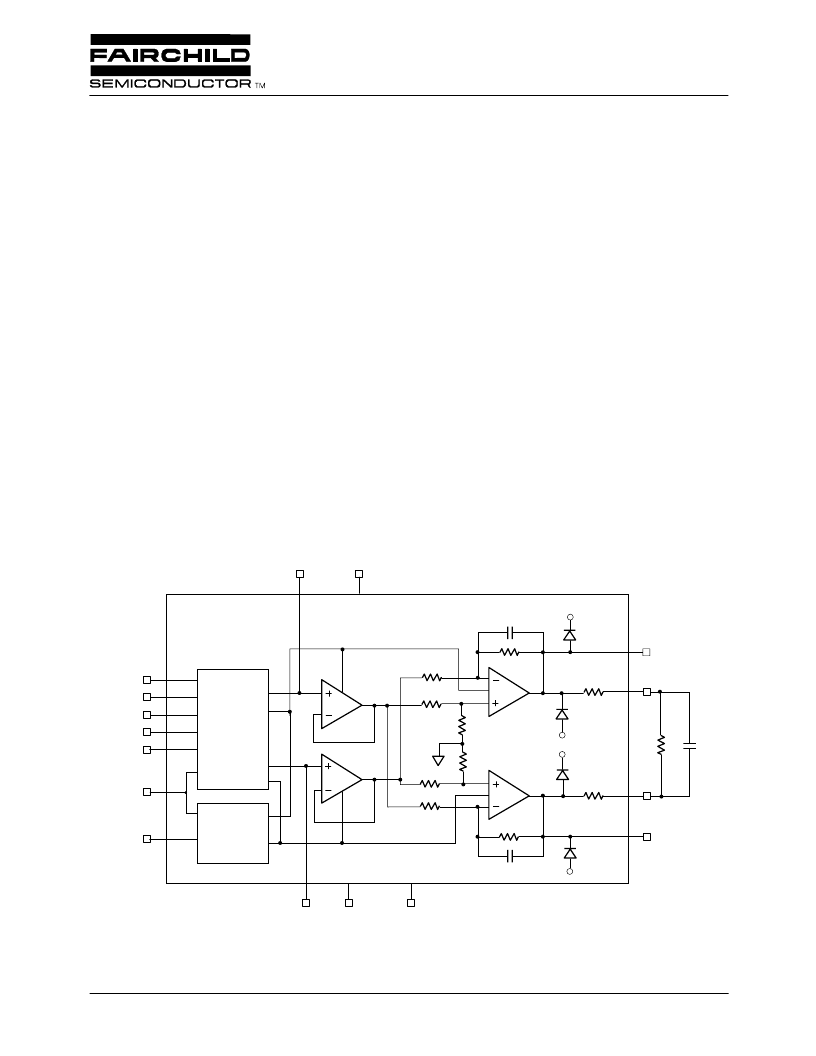
Block Diagram
65-5890A
Data (A)
Clock
Sync
V
REF
Data B
Charge Pumps
Data (A)
Clock
Sync
V
REF
Data (B)
I
SET
(B)
I
SET
(A)
V
LOGIC
Rate
Select
Cap
(A)
Cap
(B)
I
SET
(B)
I
SET
(A)
Rate
Select
Cap B
GND
V
EE
10K
10K
10K
10K
3 pF
V
EE
V
CC
V
EE
37.5
W
10K
10K
10K
3 pF
V
CC
V
CC
Cap (A)
Amp A
Out A
R
L
C
L
Out B
Amp B
37.5
W
V
LOGIC
10K
Note: Pin numbers are for the DIP package.
4
14
3
1
5
13
16
2
12
8
7
15
11
6
10
9
V
LOGIC
RM3182A
ARINC 429 Differential Line Driver
Rev. 1.0.0
相關(guān)PDF資料 |
PDF描述 |
|---|---|
| RM3183D | Line Receiver |
| RM4136FKB | Voltage-Feedback Operational Amplifier |
| RM4227BD | Voltage-Feedback Operational Amplifier |
| RM4277AD | Voltage-Feedback Operational Amplifier |
| RV4277ED | Voltage-Feedback Operational Amplifier |
相關(guān)代理商/技術(shù)參數(shù) |
參數(shù)描述 |
|---|---|
| RM3183D | 制造商:未知廠家 制造商全稱:未知廠家 功能描述:Line Receiver |
| RM3183D/883B | 制造商:未知廠家 制造商全稱:未知廠家 功能描述:Line Receiver |
| RM3183L | 制造商:未知廠家 制造商全稱:未知廠家 功能描述:Dual ARINC 429 Line Receiver |
| RM3183L/883B | 制造商:未知廠家 制造商全稱:未知廠家 功能描述:Line Receiver |
| RM3183S | 制造商:未知廠家 制造商全稱:未知廠家 功能描述:Dual ARINC 429 Line Receiver |
發(fā)布緊急采購,3分鐘左右您將得到回復(fù)。