- 您現(xiàn)在的位置:買賣IC網(wǎng) > PDF目錄385769 > RF2484 (RF MICRO DEVICES INC) DIRECT QUADRATURE MODULATOR PDF資料下載
參數(shù)資料
| 型號(hào): | RF2484 |
| 廠商: | RF MICRO DEVICES INC |
| 元件分類: | 無繩電話/電話 |
| 英文描述: | DIRECT QUADRATURE MODULATOR |
| 中文描述: | TELECOM, CELLULAR, RF AND BASEBAND CIRCUIT, PQCC16 |
| 封裝: | 4 X 4 MM, ROHS COMPLIANT, PLASTIC, QFN-16 |
| 文件頁(yè)數(shù): | 4/10頁(yè) |
| 文件大小: | 156K |
| 代理商: | RF2484 |
Preliminary
5-32
RF2484
Rev A2 010829
5
M
U
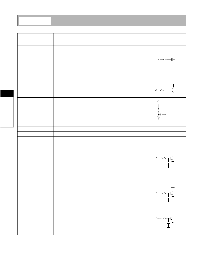
Pin
1
Function
GND
Description
Ground connection. This pin should be connected directly to the
ground plane.
Same as pin 1.
Interface Schematic
2
3
4
GND
GND
LO
Same as pin 1.
The input of the phase shifting network. This pin has an internal DC
blocking capacitor. This port is voltage-driven so matching at different
frequencies is generally not required.
Same as pin 1.
5
6
GND
VCC
Power supply. An external capacitor is needed if no other low frequency
bypass capacitor is nearby.
Power Down control. When this pin is "low," all circuits are shut off. A
"low" is typically 1.2V or less at room temperature.When this pin is
"high" (V
CC
), all circuits are operating normally. If PD is below V
CC
, out-
put power and performance will be degraded. Operating in this region
is not recommended, although it might be useful in some applications
where power control is required.
RF Output. This pin has an internal DC blocking capacitor. At some fre-
quencies, external matching may be needed to optimize output power.
A small amount of DC current may be present at this output. As a
result, if the voltage at this pin is measured using a high impedance
probe, some DC voltage may be observed at this output.
7
PD
8
RF OUT
9
10
11
12
13
GND
VCC
GND
GND
Q SIG
Same as pin 1.
Same as pin 6.
Same as pin 1.
Same as pin 1.
Baseband input to the Q mixer. This pin is DC coupled. The input drive
level determines output power and linearity performance; for better car-
rier suppression, sideband suppression, and dynamic range, the drive
level should be as high as possible to meet the required linearity perfor-
mance. The recommended DC level for this pin is 4.1V.
For optimum carrier suppression, the DC voltages on I REF, Q REF, I
SIG and Q SIG should be adjusted slightly to compensate for inherent
undesired internal DC offsets; for optimum sideband suppression,
phase and signal amplitude on IREF, Q REF, I SIG and Q SIG should
be adjusted slightly to compensate for inherent undesired internal off-
sets. See RFMD AN0001 for more detail.
Baseband input to the I mixer. This pin is DC coupled. The input drive
level determines output power and linearity performance; for better car-
rier suppression, sideband suppression, and dynamic range, the drive
level should be as high as possible to meet the required linearity perfor-
mance. The recommended DC level for this pin is 4.1V; see pin 13 for
more information.
14
I SIG
15
I REF
Reference voltage for the I mixer. This voltage should be the same as
the DC voltage supplied to the I SIG pin. A voltage of 4.1V is recom-
mended; see pin 13 for more information.
The SIG and REF inputs are inputs of a differential amplifier. Therefore
the REF and SIG inputs are interchangeable. If swapping the I SIG and
I REF pins, the Q SIG and Q REF also need to be swapped to maintain
the correct phase. It is also possible to drive the SIG and REF inputs in
a differential mode. This will increase the gain.
LO
200
PD
V
CC
RF OUT
100
1 p
V
CC
100
1 p
V
CC
100
1 p
V
CC
相關(guān)PDF資料 |
PDF描述 |
|---|---|
| RF2485 | VHF QUADRATURE MODULATOR |
| RF2486 | PCS LOW NOISE AMPLIFIER/MIXER |
| RF2488 | MULTI-MODE DUAL-BAND LNA MIXER |
| RF2489 | DUAL-BAND/TRI-MODE CDMA LOW NOISE AMPLIFIER/MIXER |
| RF2492 | DUAL-BAND LOW NOISE AMPLIFIER/MIXER |
相關(guān)代理商/技術(shù)參數(shù) |
參數(shù)描述 |
|---|---|
| RF2484_06 | 制造商:RFMD 制造商全稱:RF Micro Devices 功能描述:DIRECT QUADRATURE MODULATOR |
| RF2484_1 | 制造商:RFMD 制造商全稱:RF Micro Devices 功能描述:DIRECT QUADRATURE MODULATOR |
| RF2484PCBA-410 | 制造商:RFMD 制造商全稱:RF Micro Devices 功能描述:DIRECT QUADRATURE MODULATOR |
| RF2484PCK | 制造商:RF Micro Devices Inc 功能描述:KIT EVAL FOR RF2484 |
| RF2484TR7 | 制造商:RF Micro Devices Inc 功能描述:IC QUADRATURE MOD DUAL-BND 16QFN |
發(fā)布緊急采購(gòu),3分鐘左右您將得到回復(fù)。