- 您現(xiàn)在的位置:買賣IC網(wǎng) > PDF目錄372055 > REF02A +5V Precision VOLTAGE REFERENCE PDF資料下載
參數(shù)資料
| 型號: | REF02A |
| 英文描述: | +5V Precision VOLTAGE REFERENCE |
| 中文描述: | 5V的高精度電壓基準 |
| 文件頁數(shù): | 6/6頁 |
| 文件大小: | 111K |
| 代理商: | REF02A |
6
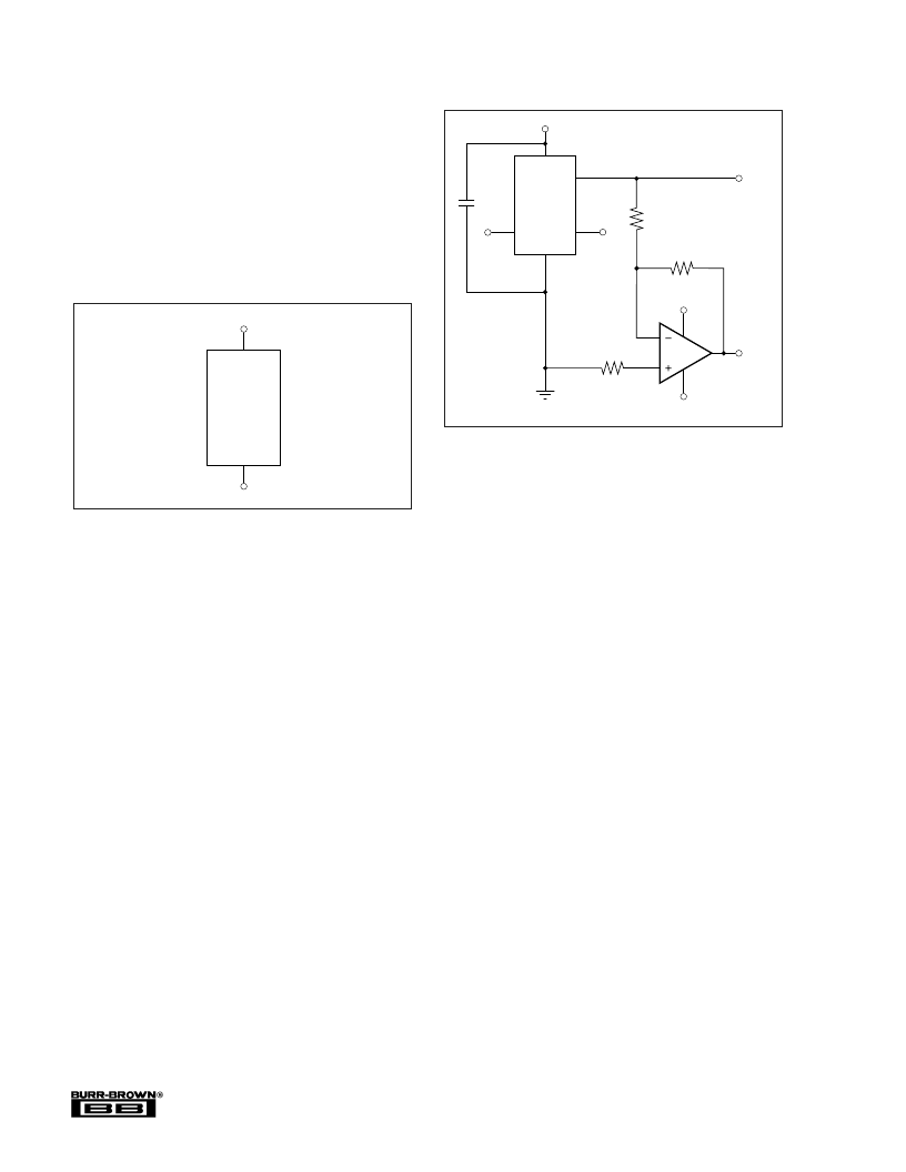
REF02
OUTPUT ADJUSTMENT
The REF02 trim terminal can be used to adjust the voltage
over a 5V
±
150mV range. This feature allows the system
designer to trim system errors by setting the reference to a
voltage other than 5V, including 5.12V
(1)
for binary applica-
tions (see circuit on page one).
Adjustment of the output does not significantly affect the
temperature performance of the device. The temperature
coefficient change is approximately 0.7ppm/
°
C for 100mV of
output adjustment.
NOTE: (1) 20mV LSB for 8-bit applications.
TYPICAL APPLICATIONS
5k
OPA177
10k
10k
–15V
+15V
–5V
–5V
Trim
GND
V
IN
3
5
4
2
REF02
0.1μF
V
O
Temp
6
FIGURE 2.
±
5V Precision Reference.
REF02
GND
2
4
–18V
+18V
V
IN
FIGURE 1. Burn-In Circuit.
REFERENCE STACKING
PROVIDES OUTSTANDING LINE REGULATION
By stacking two REF01s and one REF02, a systems designer
can achieve 5V, 15V and 25V outputs. One very important
advantage of this circuit is the near perfect line regulation at
5V and 15V outputs. This circuit can accept a 27V to 55V
change to the input with less than the noise voltage as a
change to the output voltage. (R
B
), a load bypass resistor,
supplies current (I
SY
) for the 15V regulator.
Any number of REF01s and REF02s can be stacked in this
configuration. If ten devices can be stacked in this configu-
ration, for example, ten 5V or five 10V outputs are achieved.
The line voltage may range from 100V to 130V. Care should
be exercised to insure that the total load currents do not
exceed the maximum usable current which is typically
21mA.
相關(guān)PDF資料 |
PDF描述 |
|---|---|
| REF02AU | +5V Precision VOLTAGE REFERENCE |
| REF02B | +5V Precision VOLTAGE REFERENCE |
| REF02BP | +5V Precision VOLTAGE REFERENCE |
| REF02BU | +5V Precision VOLTAGE REFERENCE |
| REF02C | +5V Precision VOLTAGE REFERENCE |
相關(guān)代理商/技術(shù)參數(shù) |
參數(shù)描述 |
|---|---|
| REF02AEJ | 制造商:Analog Devices 功能描述: |
| REF02AH | 制造商:LINER 制造商全稱:Linear Technology 功能描述:Precision Voltage References |
| REF02AH/883 | 制造商:Linear Technology 功能描述:V-Ref Precision 5V 20mA 8-Pin TO-5 |
| REF02AJ | 制造商:Maxim Integrated Products 功能描述:8 PINS TO99 PKG - Bulk |
| REF02AJ/883 | 制造商:未知廠家 制造商全稱:未知廠家 功能描述:Voltage Reference |
發(fā)布緊急采購,3分鐘左右您將得到回復(fù)。