- 您現(xiàn)在的位置:買(mǎi)賣(mài)IC網(wǎng) > PDF目錄230911 > R5F363A6DFB 16-BIT, FLASH, 20 MHz, MICROCONTROLLER, PQFP100 PDF資料下載
參數(shù)資料
| 型號(hào): | R5F363A6DFB |
| 元件分類(lèi): | 微控制器/微處理器 |
| 英文描述: | 16-BIT, FLASH, 20 MHz, MICROCONTROLLER, PQFP100 |
| 封裝: | 14 X 14 MM, 0.50 MM PITCH, PLASTIC, LQFP-100 |
| 文件頁(yè)數(shù): | 26/115頁(yè) |
| 文件大?。?/td> | 2363K |
| 代理商: | R5F363A6DFB |
第1頁(yè)第2頁(yè)第3頁(yè)第4頁(yè)第5頁(yè)第6頁(yè)第7頁(yè)第8頁(yè)第9頁(yè)第10頁(yè)第11頁(yè)第12頁(yè)第13頁(yè)第14頁(yè)第15頁(yè)第16頁(yè)第17頁(yè)第18頁(yè)第19頁(yè)第20頁(yè)第21頁(yè)第22頁(yè)第23頁(yè)第24頁(yè)第25頁(yè)當(dāng)前第26頁(yè)第27頁(yè)第28頁(yè)第29頁(yè)第30頁(yè)第31頁(yè)第32頁(yè)第33頁(yè)第34頁(yè)第35頁(yè)第36頁(yè)第37頁(yè)第38頁(yè)第39頁(yè)第40頁(yè)第41頁(yè)第42頁(yè)第43頁(yè)第44頁(yè)第45頁(yè)第46頁(yè)第47頁(yè)第48頁(yè)第49頁(yè)第50頁(yè)第51頁(yè)第52頁(yè)第53頁(yè)第54頁(yè)第55頁(yè)第56頁(yè)第57頁(yè)第58頁(yè)第59頁(yè)第60頁(yè)第61頁(yè)第62頁(yè)第63頁(yè)第64頁(yè)第65頁(yè)第66頁(yè)第67頁(yè)第68頁(yè)第69頁(yè)第70頁(yè)第71頁(yè)第72頁(yè)第73頁(yè)第74頁(yè)第75頁(yè)第76頁(yè)第77頁(yè)第78頁(yè)第79頁(yè)第80頁(yè)第81頁(yè)第82頁(yè)第83頁(yè)第84頁(yè)第85頁(yè)第86頁(yè)第87頁(yè)第88頁(yè)第89頁(yè)第90頁(yè)第91頁(yè)第92頁(yè)第93頁(yè)第94頁(yè)第95頁(yè)第96頁(yè)第97頁(yè)第98頁(yè)第99頁(yè)第100頁(yè)第101頁(yè)第102頁(yè)第103頁(yè)第104頁(yè)第105頁(yè)第106頁(yè)第107頁(yè)第108頁(yè)第109頁(yè)第110頁(yè)第111頁(yè)第112頁(yè)第113頁(yè)第114頁(yè)第115頁(yè)
REJ03B0271-0100 Rev.1.00 Sep 15, 2009
Page 18 of 113
M16C/63 Group
1. Overview
1.6
Pin Functions
Power supply: VCC2 is used to supply power to the external bus associated pins. The dual power supply configuration
allows VCC2 to interface at a different voltage than VCC1.
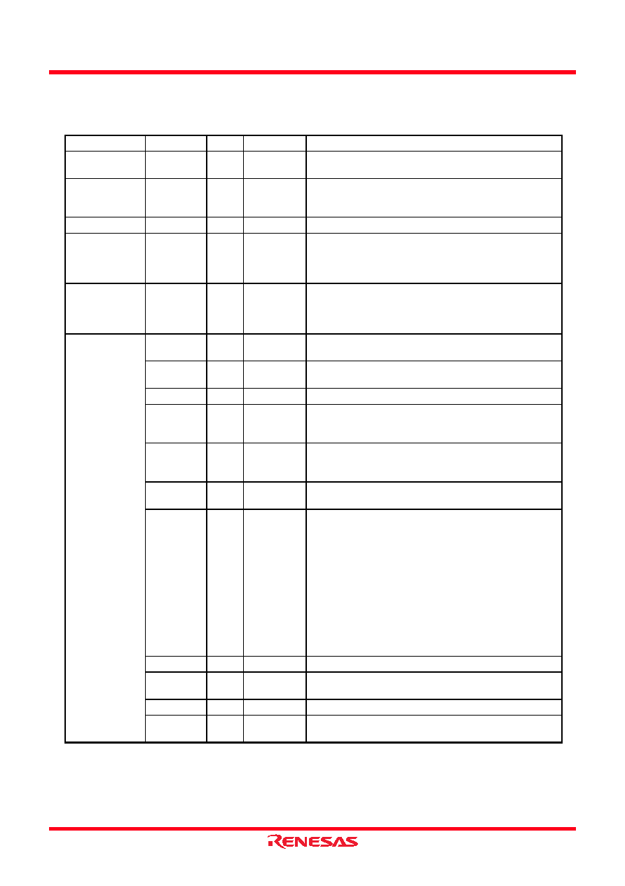
Table 1.10
Pin Functions for the 100-Pin Package (1/3)
Signal Name
Pin Name
I/O
Power Supply
Description
Power supply
input
VCC1,
VCC2, VSS
I-
Apply 1.8 to 5.5 V to pins VCC1 and VCC2 (VCC1
≥ VCC2)
and 0 V to the VSS pin.
Analog power
supply input
AVCC, AVSS
I
VCC1
This is the power supply for the A/D and D/A converters.
Connect the AVCC pin to VCC1, and connect the AVSS pin
to VSS.
Reset input
RESET
I
VCC1
Driving this pin low resets the MCU.
CNVSS
I
VCC1
Input pin to switch processor modes. After a reset, to start
operating in single-chip mode, connect the CNVSS pin to
VSS via a resistor. To start operating in microprocessor
mode, connect the pin to VCC1.
External data bus
width select input
BYTE
I
VCC1
Input pin to select the data bus of the external area. The data
bus is 16 bits when it is low, and 8 bits when it is high. This
pin must be fixed either high or low. Connect the BYTE pin to
VSS in single-chip mode.
Bus control pins
D0 to D7
I/O
VCC2
Inputs or outputs data (D0 to D7) while accessing an
external area with a separate bus.
D8 to D15
I/O
VCC2
Inputs or outputs data (D8 to D15) while accessing an
external area with a 16-bit separate bus.
A0 to A19
O
VCC2
Outputs address bits A0 to A19.
A0/D0 to
A7/D7
I/O
VCC2
Inputs or outputs data (D0 to D7) and outputs address bits
(A0 to A7) by timesharing, while accessing an external area
with an 8-bit multiplexed bus.
A1/D0 to
A8/D7
I/O
VCC2
Inputs or outputs data (D0 to D7) and outputs address bits
(A1 to A8) by timesharing, while accessing an external area
with a 16-bit multiplexed bus.
CS0 to CS3
O
VCC2
Outputs chip-select signals
CS0 to CS3 to specify an
external area.
WRL/WR
WRH/BHE
RD
O
VCC2
Outputs
WRL, WRH, (WR, BHE), and RD signals. WRL and
WRH can be switched with BHE and WR.
WRL, WRH, and RD selected
If the external data bus is 16 bits, data is written to an even
address in an external area when
WRL is driven low. Data
is written to an odd address when
WRH is driven low. Data
is read when
RD is driven low.
WR, BHE, and RD selected
Data is written to an external area when
WR is driven low.
Data in an external area is read when
RD is driven low. An
odd address is accessed when
BHE is driven low. Select
WR, BHE, and RD when using an 8-bit external data bus.
ALE
O
VCC2
Outputs ALE signal to latch address.
HOLD
I
VCC2
The MCU is placed in a hold state while the
HOLD pin is
driven low.
HLDA
O
VCC2
In a hold state,
HLDA outputs a low-level signal.
RDY
I
VCC2
The MCU bus is placed in a wait state while the
RDY pin is
driven low.
相關(guān)PDF資料 |
PDF描述 |
|---|---|
| R5F363A6NFA | 16-BIT, FLASH, 20 MHz, MICROCONTROLLER, PQFP100 |
| R5F363A6NFB | 16-BIT, FLASH, 20 MHz, MICROCONTROLLER, PQFP100 |
| RTC-6583 | REAL TIME CLOCK, PDSO24 |
| R5F61644N50FPV | 32-BIT, FLASH, 50 MHz, MICROCONTROLLER, PQFP144 |
| R5F3650EDFA | MICROCONTROLLER, PQFP100 |
相關(guān)代理商/技術(shù)參數(shù) |
參數(shù)描述 |
|---|---|
| R5F363A6NFA | 制造商:RENESAS 制造商全稱(chēng):Renesas Technology Corp 功能描述:RENESAS MCU |
| R5F363A6NFA_11 | 制造商:RENESAS 制造商全稱(chēng):Renesas Technology Corp 功能描述:This MCU consumes low power, and supports operating modes |
| R5F363A6NFB | 制造商:Renesas Electronics Corporation 功能描述: |
| R5F363A6NFB#U0 | 制造商:Renesas Electronics Corporation 功能描述: |
| R5F363A6NLG | 制造商:RENESAS 制造商全稱(chēng):Renesas Technology Corp 功能描述:This MCU consumes low power, and supports operating modes |
發(fā)布緊急采購(gòu),3分鐘左右您將得到回復(fù)。