- 您現(xiàn)在的位置:買賣IC網(wǎng) > PDF目錄269904 > QS29FCT2521CP (QUALITY SEMICONDUCTOR INC) 8-BIT, DSP-PIPELINE REGISTER, PDIP24 PDF資料下載
參數(shù)資料
| 型號: | QS29FCT2521CP |
| 廠商: | QUALITY SEMICONDUCTOR INC |
| 元件分類: | 數(shù)字信號處理外設 |
| 英文描述: | 8-BIT, DSP-PIPELINE REGISTER, PDIP24 |
| 封裝: | DIP-24 |
| 文件頁數(shù): | 4/6頁 |
| 文件大小: | 43K |
| 代理商: | QS29FCT2521CP |
4
QUALITY SEMICONDUCTOR, INC.
MDSL-00002-02
QS29FCT520T, 521T, 2520T, 2521T
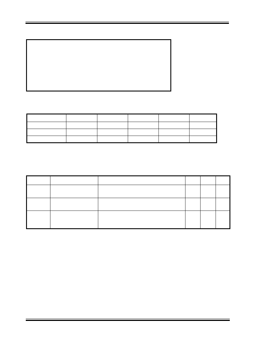
Pins
SOIC
QSOP
PDIP
ZIP
Unit
1-11, 13, 22, 23
4
5
7
pF
14-21
6
7
9
pF
—
8
9
10
pF
Note: Capacitance is characterized but not tested.
POWER SUPPLY CHARACTERISTICS
Symbol
Parameter
Test Conditions(1)
Min
Max
Unit
Icc
Quiescent Power
Vcc = Max., freq = 0
—
1.5
mA
Supply Current
0V
≤ VIN ≤ 0.2V or Vcc-0.2V ≤ VIN ≤ Vcc
Icc
Supply Current per
Vcc = Max., VIN = 3.4V, freq = 0(2)
—
2.0
mA
Input @ TTL HIGH
Qccd
Supply Current per
Vcc = Max., Outputs Open and Enabled
—
0.25
mA/
Input per MHz
One Bit Toggling @ 50% Duty Cycle
MHz
Other Inputs at GND or Vcc(3,4)
Notes:
1. For conditions shown as Min. or Max., use the appropriate values specified under DC specifications.
2. Per TTL driven input (VIN = 3.4V).
3. For flip-flops, Qccd is measured by switching one of the data input pins so that the output changes every clock cycle.
This is a measurement of device power consumption only and does not include power to drive load capacitance or tester
capacitance. This parameter is guaranteed by design but not tested.
4. Ic can be computed using the above parameters as explained in the Technical Overview section.
ABSOLUTE MAXIMUM RATINGS
Supply Voltage to Ground .............................................. –0.5V to +7.0V
DC Output Voltage VOUT ............................................... –0.5V to +7.0V
DC Input Voltage VIN ....................................................... –0.5V to +7.0V
AC Input Voltage (for a pulse width
≤ 20 ns) ................................. –3.0V
DC Input Diode Current with VIN < 0 ........................................... –20 mA
DC Output Diode Current with VOUT < 0 ..................................... –50 mA
DC Output Current Max. Sink Current/Pin ................................. 120 mA
Maximum Power Dissipation .................................................... 0.5 watts
TSTG Storage Temperature ............................................. –65
° to +150°C
CAPACITANCE
TA = 25
°C, f = 1 MHz, VIN = 0V, VOUT = 0V
Note:
Stresses greater than
those listed under ABSOLUTE
MAXIMUM RATINGS may
cause permanent damage to
this device resulting in func-
tional or reliability type failures.
相關PDF資料 |
PDF描述 |
|---|---|
| QL5232-33APB456I | PCI BUS CONTROLLER, PBGA456 |
| QL5820-33BPTN196I | PCI BUS CONTROLLER, PBGA196 |
| QL5820-66CPFN144C | PCI BUS CONTROLLER, PQFP144 |
| QL5840-33BPTN280M | PCI BUS CONTROLLER, PBGA280 |
| QL5842-33APS484I | PCI BUS CONTROLLER, PBGA484 |
相關代理商/技術參數(shù) |
參數(shù)描述 |
|---|---|
| QS29FCT2521CTHB | 制造商:未知廠家 制造商全稱:未知廠家 功能描述:Pipeline Register |
| QS29FCT2521CTP | 制造商:未知廠家 制造商全稱:未知廠家 功能描述:Pipeline Register |
| QS29FCT2521CTQ | 制造商:未知廠家 制造商全稱:未知廠家 功能描述:Pipeline Register |
| QS29FCT2521CTSO | 制造商:Rochester Electronics LLC 功能描述:- Bulk 制造商:Integrated Device Technology Inc 功能描述: |
| QS29FCT2521CTZ | 制造商:未知廠家 制造商全稱:未知廠家 功能描述:Pipeline Register |
發(fā)布緊急采購,3分鐘左右您將得到回復。