- 您現(xiàn)在的位置:買賣IC網(wǎng) > PDF目錄69257 > PTPS659106A1RSLR (TEXAS INSTRUMENTS INC) POWER SUPPLY SUPPORT CKT, PQCC48 PDF資料下載
參數(shù)資料
| 型號: | PTPS659106A1RSLR |
| 廠商: | TEXAS INSTRUMENTS INC |
| 元件分類: | 電源管理 |
| 英文描述: | POWER SUPPLY SUPPORT CKT, PQCC48 |
| 封裝: | 6 X 6 MM, 1 MM HEIGHT, GREEN, PLASTIC,VQFN-48 |
| 文件頁數(shù): | 28/89頁 |
| 文件大小: | 941K |
| 代理商: | PTPS659106A1RSLR |
第1頁第2頁第3頁第4頁第5頁第6頁第7頁第8頁第9頁第10頁第11頁第12頁第13頁第14頁第15頁第16頁第17頁第18頁第19頁第20頁第21頁第22頁第23頁第24頁第25頁第26頁第27頁當前第28頁第29頁第30頁第31頁第32頁第33頁第34頁第35頁第36頁第37頁第38頁第39頁第40頁第41頁第42頁第43頁第44頁第45頁第46頁第47頁第48頁第49頁第50頁第51頁第52頁第53頁第54頁第55頁第56頁第57頁第58頁第59頁第60頁第61頁第62頁第63頁第64頁第65頁第66頁第67頁第68頁第69頁第70頁第71頁第72頁第73頁第74頁第75頁第76頁第77頁第78頁第79頁第80頁第81頁第82頁第83頁第84頁第85頁第86頁第87頁第88頁第89頁
PRODUCTPREVIEW
SWCS046-016
SCLSR_EN1
VDIG1
1.2 V
VPLL
1.8 V
SCLSR_EN2
NRESPWON
TdVEN
TdEN
Switch-on sequence
Swtich-off sequence
Device on
TdEN
TdSOFF2
TdEN
Low-power mode
SWCS046-017
SCLSR_EN2
VDD2/VFB2
VDD1/VFB1
1.2 V
SCLSR_EN1
NRESPWON
Low-power mode
PFM (pulse skipping) mode
Switch-on sequence
Swtich-off sequence
Device on
PWM mode
SW1
TdOEN
0 V
TdVDDEN
TdOEN
TdEN
3.3 V
TdVDDEN
TdSOFF2
TdEN
SWCS046C – MARCH 2010 – REVISED JUNE 2010
www.ti.com
Table 7. Device Turn-on/off with Rising/Falling Input Voltage, Timing Characteristics (continued)
PARAMETER
TEST CONDITIONS
MIN
TYP
MAX
UNIT
tdONPWHOLD: delay to set high PWRHOLD signal or
tPDINT1 –
DEV_ON control bit after NRESPWON released to
tDSONT =
ms
keep on the supplies
984
TdbVMBDCH: Main Battery voltage = VMBDCH
3 × tCK32k
4 × tCK32k
s
threshold to INT1 falling edge delay
= 94
= 125
TdbVMBLO: Main Battery voltage = VMBLO threshold
3 × tCK32k
4 × tCK32k
s
to NRESPWON falling edge delay
= 94
= 125
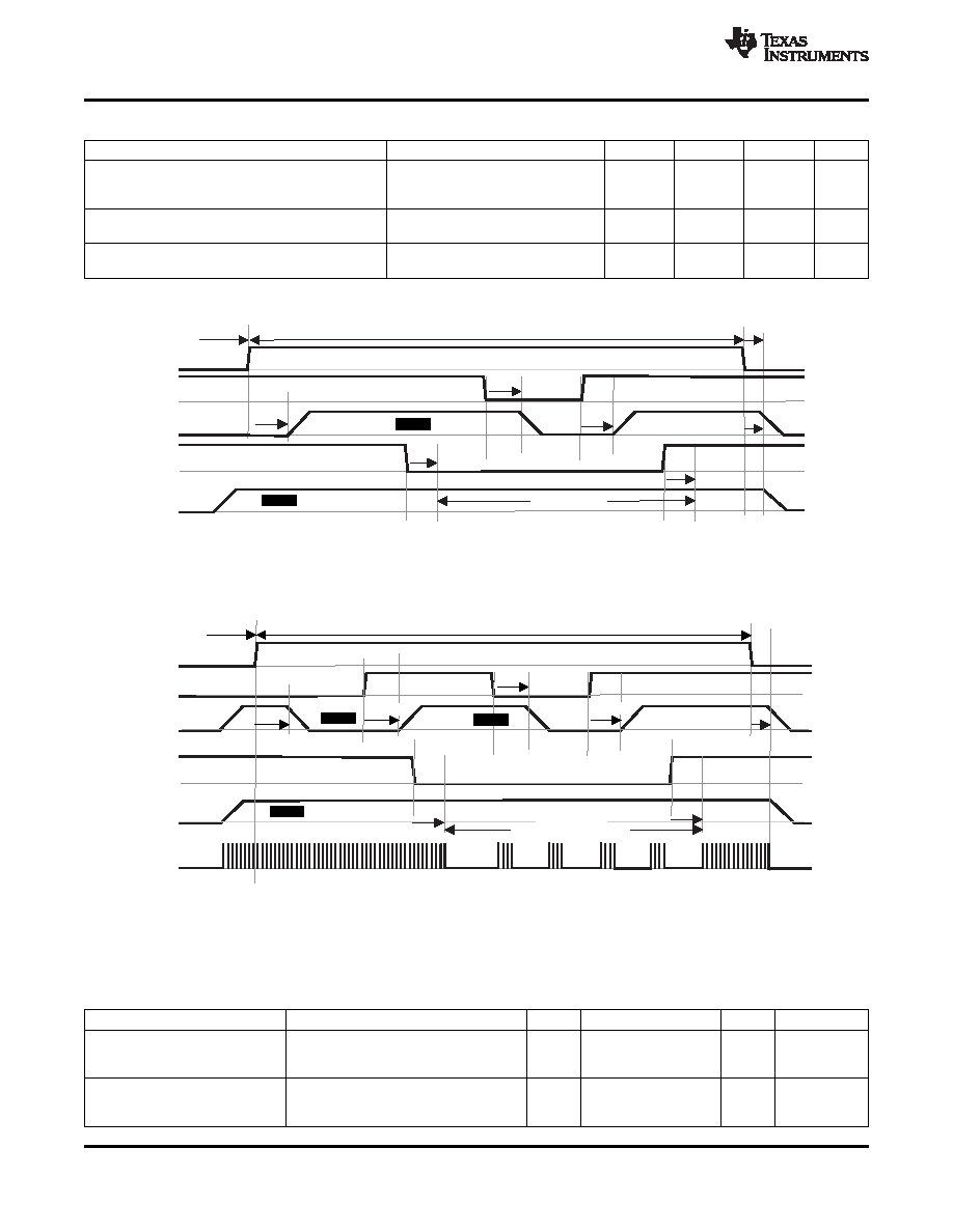
Power supplies state control though the SCLSR_EN1 and SDASR_EN2 signals.
Figure 7. LDO Type Supplies State Control Though SCLSR_EN1 and SCLSR_EN2
Note: Register setting: VDIG1_EN1 = 1, VPLL_EN2 = 1, and VPLL_KEEPON = 1
Figure 8. VDD1 and VDD2 Supplies State Control Though SCLSR_EN1 and SCLSR_EN2
Note: Register setting: VDD2_EN2 = 1, VDD1_EN1 = 1, VDD1_KEEPON = 1, VDD1_PSKIP = 0, and SEL[6:0] =
hex00 in VDD2_SR_REG
Table 8. Supplies State Control Though SCLSR_EN1 and SCLSR_EN2 Timing Characteristics
Parameter
TEST CONDITIONS
MIN
TYP
MAX
UNIT
tdEN: NREPSWON to supply state
change delay, SCLSR_EN1 or
0
ms
SCLSR_EN2 driven
tdEN: SCLSR_EN1 or
SCLSR_EN2 edge to supply state
1 × tCK32k = 31
s
change delay
34
Copyright 2010, Texas Instruments Incorporated
相關(guān)PDF資料 |
PDF描述 |
|---|---|
| PTPS659102A1RSLR | POWER SUPPLY SUPPORT CKT, PQCC48 |
| PTPS659104A1RSLR | POWER SUPPLY SUPPORT CKT, PQCC48 |
| PTPS659107A1RSL | POWER SUPPLY SUPPORT CKT, PQCC48 |
| PTPS659105A1RSLR | POWER SUPPLY SUPPORT CKT, PQCC48 |
| PTPS659103A1RSL | POWER SUPPLY SUPPORT CKT, PQCC48 |
相關(guān)代理商/技術(shù)參數(shù) |
參數(shù)描述 |
|---|---|
| PTPS659109A1RSL | 制造商:Texas Instruments 功能描述: |
| PTPS6591102A2ZRCR | 制造商:TI 功能描述:TPS65911 |
| PTPS6591102ZRC | 制造商:TI 功能描述:TPS65911 |
| PTPS6591104A2ZRCR | 制造商:TI 功能描述:TPS65911 |
| PTPS659110A2ZRC | 制造商:TI 功能描述:TPS65911 |
發(fā)布緊急采購,3分鐘左右您將得到回復(fù)。