- 您現(xiàn)在的位置:買賣IC網(wǎng) > PDF目錄268247 > PSD813F4-70M (STMICROELECTRONICS) 128K X 8 FLASH, 27 I/O, PIA-GENERAL PURPOSE, PQFP52 PDF資料下載
參數(shù)資料
| 型號(hào): | PSD813F4-70M |
| 廠商: | STMICROELECTRONICS |
| 元件分類: | 微控制器/微處理器 |
| 英文描述: | 128K X 8 FLASH, 27 I/O, PIA-GENERAL PURPOSE, PQFP52 |
| 封裝: | PLASTIC, QFP-52 |
| 文件頁(yè)數(shù): | 22/103頁(yè) |
| 文件大小: | 1180K |
| 代理商: | PSD813F4-70M |
第1頁(yè)第2頁(yè)第3頁(yè)第4頁(yè)第5頁(yè)第6頁(yè)第7頁(yè)第8頁(yè)第9頁(yè)第10頁(yè)第11頁(yè)第12頁(yè)第13頁(yè)第14頁(yè)第15頁(yè)第16頁(yè)第17頁(yè)第18頁(yè)第19頁(yè)第20頁(yè)第21頁(yè)當(dāng)前第22頁(yè)第23頁(yè)第24頁(yè)第25頁(yè)第26頁(yè)第27頁(yè)第28頁(yè)第29頁(yè)第30頁(yè)第31頁(yè)第32頁(yè)第33頁(yè)第34頁(yè)第35頁(yè)第36頁(yè)第37頁(yè)第38頁(yè)第39頁(yè)第40頁(yè)第41頁(yè)第42頁(yè)第43頁(yè)第44頁(yè)第45頁(yè)第46頁(yè)第47頁(yè)第48頁(yè)第49頁(yè)第50頁(yè)第51頁(yè)第52頁(yè)第53頁(yè)第54頁(yè)第55頁(yè)第56頁(yè)第57頁(yè)第58頁(yè)第59頁(yè)第60頁(yè)第61頁(yè)第62頁(yè)第63頁(yè)第64頁(yè)第65頁(yè)第66頁(yè)第67頁(yè)第68頁(yè)第69頁(yè)第70頁(yè)第71頁(yè)第72頁(yè)第73頁(yè)第74頁(yè)第75頁(yè)第76頁(yè)第77頁(yè)第78頁(yè)第79頁(yè)第80頁(yè)第81頁(yè)第82頁(yè)第83頁(yè)第84頁(yè)第85頁(yè)第86頁(yè)第87頁(yè)第88頁(yè)第89頁(yè)第90頁(yè)第91頁(yè)第92頁(yè)第93頁(yè)第94頁(yè)第95頁(yè)第96頁(yè)第97頁(yè)第98頁(yè)第99頁(yè)第100頁(yè)第101頁(yè)第102頁(yè)第103頁(yè)
25/103
PSD8XXF2/3/4/5
Specific Features
Flash Memory Sector Protect. Each
primary
and secondary Flash memory sector can be sepa-
rately protected against Program and Erase cy-
cles. Sector Protection provides additional data
security because it disables all Program or Erase
cycles. This mode can be activated through the
JTAG Port or a Device Programmer.
Sector protection can be selected for each sector
using the PSDsoft Express Configuration pro-
gram. This automatically protects selected sectors
when the device is programmed through the JTAG
Port or a Device Programmer. Flash memory sec-
tors can be unprotected to allow updating of their
contents using the JTAG Port or a Device Pro-
grammer. The MCU can read (but cannot change)
the sector protection bits.
Any attempt to program or erase a protected Flash
memory sector is ignored by the device. The Verify
operation results in a READ of the protected data.
This allows a guarantee of the retention of the Pro-
tection status.
The sector protection status can be read by the
MCU through the Flash memory protection and
PSD/EE protection registers (in the CSIOP block).
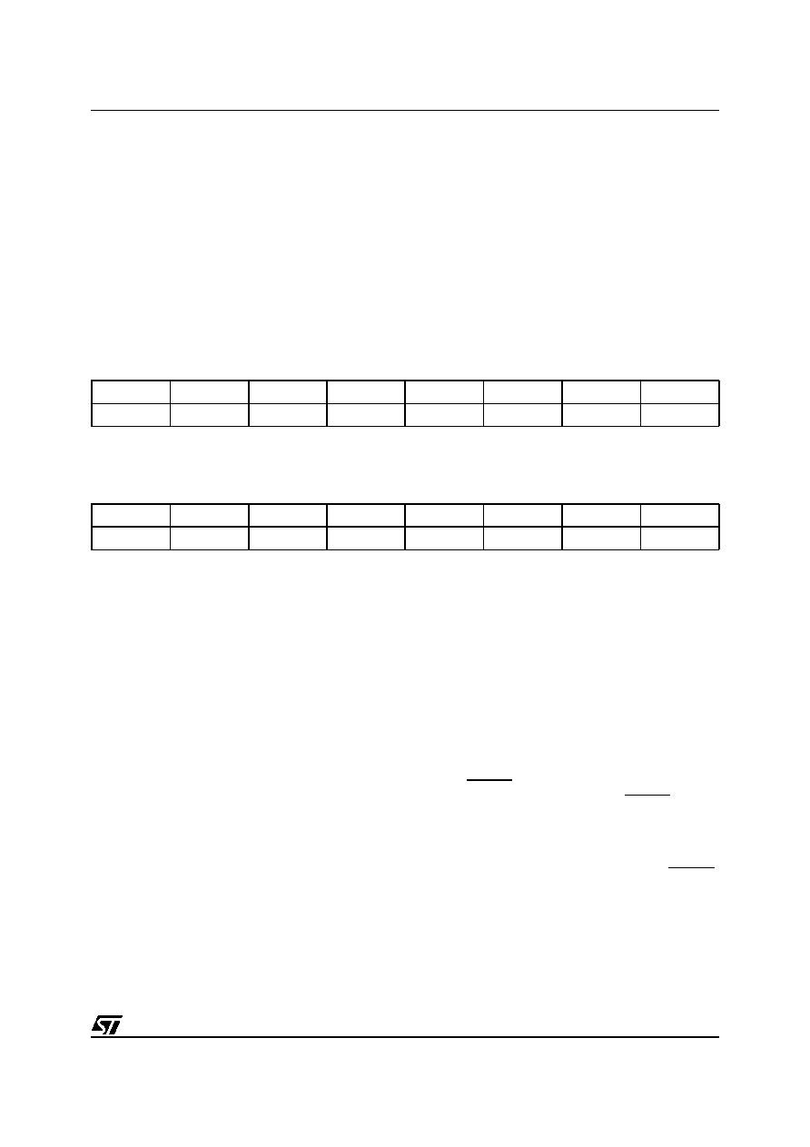
Table 10. Sector Protection/Security Bit Definition – Flash Protection Register
Note: 1. Bit Definitions:
Sec<i>_Prot 1 = Primary Flash memory or secondary Flash memory Sector <i> is write protected.
Sec<i>_Prot 0 = Primary Flash memory or secondary Flash memory Sector <i> is not write protected.
Table 11. Sector Protection/Security Bit Definition – PSD/EE Protection Register
Note: 1. Bit Definitions:
Sec<i>_Prot 1 = Secondary Flash memory Sector <i> is write protected.
Sec<i>_Prot 0 = Secondary Flash memory Sector <i> is not write protected.
Security_Bit 0 = Security Bit in device has not been set.
1 = Security Bit in device has been set.
Reset Flash. The Reset Flash instruction con-
sists of one WRITE cycle (see Table 8). It can also
be optionally preceded by the standard two
WRITE decoding cycles (writing AAh to 555h and
55h to AAAh). It must be executed after:
– Reading the Flash Protection Status or Flash ID
– An Error condition has occurred (and the device
has set the Error Flag (DQ5) bit to 1) during a
Flash memory Program or Erase cycle.
On the PSD813F2/3/4/5, the Reset Flash instruc-
tion puts the Flash memory back into normal
READ Mode. It may take the Flash memory up to
a few milliseconds to complete the Reset cycle.
The Reset Flash instruction is ignored when it is is-
sued during a Program or Bulk Erase cycle of the
Flash memory. The Reset Flash instruction aborts
any on-going Sector Erase cycle, and returns the
Flash memory to the normal READ Mode within a
few milliseconds.
On the PSD83xF2 or PSD85xF2, the Reset Flash
instruction puts the Flash memory back into nor-
mal READ Mode. If an Error condition has oc-
curred (and the device has set the Error Flag
(DQ5) bit to 1) the Flash memory is put back into
normal READ Mode within 25
s of the Reset
Flash instruction having been issued. The Reset
Flash instruction is ignored when it is issued dur-
ing a Program or Bulk Erase cycle of the Flash
memory. The Reset Flash instruction aborts any
on-going Sector Erase cycle, and returns the
Flash memory to the normal READ Mode within
25
s.
Reset (RESET) Signal (on the PSD83xF2 and
PSD85xF2). A pulse on Reset (RESET) aborts
any cycle that is in progress, and resets the Flash
memory to the READ Mode. When the reset oc-
curs during a Program or Erase cycle, the Flash
memory takes up to 25
s to return to the READ
Mode. It is recommended that the Reset (RESET)
pulse (except for Power On Reset, as described
on page 63) be at least 25
s so that the Flash
memory is always ready for the MCU to fetch the
bootstrap instructions after the Reset cycle is com-
plete.
Bit 7
Bit 6
Bit 5
Bit 4
Bit 3
Bit 2
Bit 1
Bit 0
Sec7_Prot
Sec6_Prot
Sec5_Prot
Sec4_Prot
Sec3_Prot
Sec2_Prot
Sec1_Prot
Sec0_Prot
Bit 7
Bit 6
Bit 5
Bit 4
Bit 3
Bit 2
Bit 1
Bit 0
Security_Bit
not used
Sec3_Prot
Sec2_Prot
Sec1_Prot
Sec0_Prot
相關(guān)PDF資料 |
PDF描述 |
|---|---|
| PIC16C57C-04E/SS | 8-BIT, OTPROM, 4 MHz, RISC MICROCONTROLLER, PDSO28 |
| PIC16LC55A-04/SP | 8-BIT, OTPROM, 4 MHz, RISC MICROCONTROLLER, PDIP28 |
| PIC16LC57CT-04/SS | 8-BIT, OTPROM, 4 MHz, RISC MICROCONTROLLER, PDSO28 |
| P8-186 | 1850 MHz - 1990 MHz PARABOLIC ANTENNA, 30.5 dBi GAIN, 4.4 deg 3dB BEAMWIDTH |
| PSTG0-2400HS | MOBILE STATION ANTENNA |
相關(guān)代理商/技術(shù)參數(shù) |
參數(shù)描述 |
|---|---|
| PSD813F4A-90J | 功能描述:SPLD - 簡(jiǎn)單可編程邏輯器件 U 511-PSD813F2A-90J RoHS:否 制造商:Texas Instruments 邏輯系列:TICPAL22V10Z 大電池?cái)?shù)量:10 最大工作頻率:66 MHz 延遲時(shí)間:25 ns 工作電源電壓:4.75 V to 5.25 V 電源電流:100 uA 最大工作溫度:+ 75 C 最小工作溫度:0 C 安裝風(fēng)格:Through Hole 封裝 / 箱體:DIP-24 |
| PSD813F4A-90M | 功能描述:SPLD - 簡(jiǎn)單可編程邏輯器件 U 511-PSD813F2A-90M RoHS:否 制造商:Texas Instruments 邏輯系列:TICPAL22V10Z 大電池?cái)?shù)量:10 最大工作頻率:66 MHz 延遲時(shí)間:25 ns 工作電源電壓:4.75 V to 5.25 V 電源電流:100 uA 最大工作溫度:+ 75 C 最小工作溫度:0 C 安裝風(fēng)格:Through Hole 封裝 / 箱體:DIP-24 |
| PSD813F4VA-15J | 功能描述:SPLD - 簡(jiǎn)單可編程邏輯器件 U 511-PSD813F2VA-15J RoHS:否 制造商:Texas Instruments 邏輯系列:TICPAL22V10Z 大電池?cái)?shù)量:10 最大工作頻率:66 MHz 延遲時(shí)間:25 ns 工作電源電壓:4.75 V to 5.25 V 電源電流:100 uA 最大工作溫度:+ 75 C 最小工作溫度:0 C 安裝風(fēng)格:Through Hole 封裝 / 箱體:DIP-24 |
| PSD813F4VA-15U | 功能描述:SPLD - 簡(jiǎn)單可編程邏輯器件 U 511-PSD813F2VA-15U RoHS:否 制造商:Texas Instruments 邏輯系列:TICPAL22V10Z 大電池?cái)?shù)量:10 最大工作頻率:66 MHz 延遲時(shí)間:25 ns 工作電源電壓:4.75 V to 5.25 V 電源電流:100 uA 最大工作溫度:+ 75 C 最小工作溫度:0 C 安裝風(fēng)格:Through Hole 封裝 / 箱體:DIP-24 |
| PSD813F5-12JI | 制造商:WSI 功能描述: |
發(fā)布緊急采購(gòu),3分鐘左右您將得到回復(fù)。