- 您現(xiàn)在的位置:買(mǎi)賣(mài)IC網(wǎng) > PDF目錄368152 > PSD411A1-C-90JI (意法半導(dǎo)體) High Speed CMOS Logic Dual 2-to-4 Line Decoders/Demultiplexers 16-SOIC -55 to 125 PDF資料下載
參數(shù)資料
| 型號(hào): | PSD411A1-C-90JI |
| 廠(chǎng)商: | 意法半導(dǎo)體 |
| 英文描述: | High Speed CMOS Logic Dual 2-to-4 Line Decoders/Demultiplexers 16-SOIC -55 to 125 |
| 中文描述: | 低成本現(xiàn)場(chǎng)可編程微控制器外圍設(shè)備 |
| 文件頁(yè)數(shù): | 75/123頁(yè) |
| 文件大小: | 657K |
| 代理商: | PSD411A1-C-90JI |
第1頁(yè)第2頁(yè)第3頁(yè)第4頁(yè)第5頁(yè)第6頁(yè)第7頁(yè)第8頁(yè)第9頁(yè)第10頁(yè)第11頁(yè)第12頁(yè)第13頁(yè)第14頁(yè)第15頁(yè)第16頁(yè)第17頁(yè)第18頁(yè)第19頁(yè)第20頁(yè)第21頁(yè)第22頁(yè)第23頁(yè)第24頁(yè)第25頁(yè)第26頁(yè)第27頁(yè)第28頁(yè)第29頁(yè)第30頁(yè)第31頁(yè)第32頁(yè)第33頁(yè)第34頁(yè)第35頁(yè)第36頁(yè)第37頁(yè)第38頁(yè)第39頁(yè)第40頁(yè)第41頁(yè)第42頁(yè)第43頁(yè)第44頁(yè)第45頁(yè)第46頁(yè)第47頁(yè)第48頁(yè)第49頁(yè)第50頁(yè)第51頁(yè)第52頁(yè)第53頁(yè)第54頁(yè)第55頁(yè)第56頁(yè)第57頁(yè)第58頁(yè)第59頁(yè)第60頁(yè)第61頁(yè)第62頁(yè)第63頁(yè)第64頁(yè)第65頁(yè)第66頁(yè)第67頁(yè)第68頁(yè)第69頁(yè)第70頁(yè)第71頁(yè)第72頁(yè)第73頁(yè)第74頁(yè)當(dāng)前第75頁(yè)第76頁(yè)第77頁(yè)第78頁(yè)第79頁(yè)第80頁(yè)第81頁(yè)第82頁(yè)第83頁(yè)第84頁(yè)第85頁(yè)第86頁(yè)第87頁(yè)第88頁(yè)第89頁(yè)第90頁(yè)第91頁(yè)第92頁(yè)第93頁(yè)第94頁(yè)第95頁(yè)第96頁(yè)第97頁(yè)第98頁(yè)第99頁(yè)第100頁(yè)第101頁(yè)第102頁(yè)第103頁(yè)第104頁(yè)第105頁(yè)第106頁(yè)第107頁(yè)第108頁(yè)第109頁(yè)第110頁(yè)第111頁(yè)第112頁(yè)第113頁(yè)第114頁(yè)第115頁(yè)第116頁(yè)第117頁(yè)第118頁(yè)第119頁(yè)第120頁(yè)第121頁(yè)第122頁(yè)第123頁(yè)
PSD4XX Famly
72
10.0
Page
Register
The PSD4XX has a programmable security bit which offers protection from unauthorized
duplication. When the security bit is set, the contents of the EPROM, the PSD4XX
non-volatile configuration bits and ZPLD data cannot be read by EPROM programmers.
The security bit is set through the PSDsoft Software and is embedded in the compiled
output file. The security bit is UV erasable and a secured part can be erased and then
re-programmed.
11.0
Security
Protection
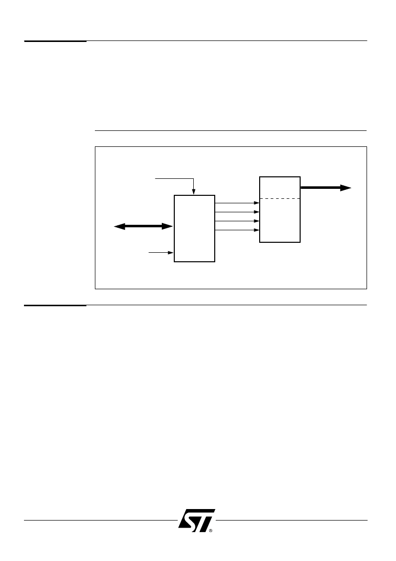
Figure 35. Page Register
DPLD
RS0
GPLD
ZPLD
ES0 – 3
PGR0
PGR1
PGR2
PGR3
R/W
D0
D0 – D3
D1
D2
D3
Q0
Q1
Q2
Q3
PAGE
REG.
RESET
The Page Register is 4 bits wide and consists of four D flip flops.The outputs of the Register
(PGR0 – PGR3) are connected to the input bus of the ZPLD. By including the four outputs
as inputs to the DPLD, the addressing capability of the microcontroller is increased by a
factor of 16.
Figure 37 shows the Page Register block diagram. Inputs to the four flip flops are connected
to data bus D0-D3. The output of the Register can be read by the microcontroller. The
Register can operate as an independent register to the microcontroller if page mode is not
implemented.
相關(guān)PDF資料 |
PDF描述 |
|---|---|
| PSD411A1-C-90UI | High Speed CMOS Logic Hex Schmitt-Triggered Inverters 14-PDIP -55 to 125 |
| PSD411A2-C-70J | High Speed CMOS Logic Hex Schmitt-Triggered Inverters 14-SOIC -55 to 125 |
| PSD411A2-C-70L | High Speed CMOS Logic Hex Schmitt-Triggered Inverters 14-SOIC -55 to 125 |
| PSD411A2-C-70U | High Speed CMOS Logic Hex Schmitt-Triggered Inverters 14-SOIC -55 to 125 |
| PSD411A2-C-90JI | High Speed CMOS Logic Hex Schmitt-Triggered Inverters 14-SOIC -55 to 125 |
相關(guān)代理商/技術(shù)參數(shù) |
參數(shù)描述 |
|---|---|
| PSD411A1-C-90UI | 制造商:STMICROELECTRONICS 制造商全稱(chēng):STMicroelectronics 功能描述:Low Cost Field Programmable Microcontroller Peripherals |
| PSD411A2 | 制造商:STMICROELECTRONICS 制造商全稱(chēng):STMicroelectronics 功能描述:Low Cost Field Programmable Microcontroller Peripherals |
| PSD411A2-12J | 制造商:未知廠(chǎng)家 制造商全稱(chēng):未知廠(chǎng)家 功能描述:Field-Programmable Peripheral |
| PSD411A2-12JI | 制造商:未知廠(chǎng)家 制造商全稱(chēng):未知廠(chǎng)家 功能描述:Field-Programmable Peripheral |
| PSD411A2-12LI | 制造商:未知廠(chǎng)家 制造商全稱(chēng):未知廠(chǎng)家 功能描述:Field-Programmable Peripheral |
發(fā)布緊急采購(gòu),3分鐘左右您將得到回復(fù)。