- 您現(xiàn)在的位置:買賣IC網(wǎng) > PDF目錄368096 > PPC440GX-3CF533CZ (APPLIEDMICRO INC) Power PC 440GX Embedded Processor PDF資料下載
參數(shù)資料
| 型號: | PPC440GX-3CF533CZ |
| 廠商: | APPLIEDMICRO INC |
| 元件分類: | 微控制器/微處理器 |
| 英文描述: | Power PC 440GX Embedded Processor |
| 中文描述: | 32-BIT, 533 MHz, RISC PROCESSOR, CBGA552 |
| 封裝: | 25 X 25 MM, CERAMIC, FBGA-552 |
| 文件頁數(shù): | 53/93頁 |
| 文件大小: | 794K |
| 代理商: | PPC440GX-3CF533CZ |
第1頁第2頁第3頁第4頁第5頁第6頁第7頁第8頁第9頁第10頁第11頁第12頁第13頁第14頁第15頁第16頁第17頁第18頁第19頁第20頁第21頁第22頁第23頁第24頁第25頁第26頁第27頁第28頁第29頁第30頁第31頁第32頁第33頁第34頁第35頁第36頁第37頁第38頁第39頁第40頁第41頁第42頁第43頁第44頁第45頁第46頁第47頁第48頁第49頁第50頁第51頁第52頁當(dāng)前第53頁第54頁第55頁第56頁第57頁第58頁第59頁第60頁第61頁第62頁第63頁第64頁第65頁第66頁第67頁第68頁第69頁第70頁第71頁第72頁第73頁第74頁第75頁第76頁第77頁第78頁第79頁第80頁第81頁第82頁第83頁第84頁第85頁第86頁第87頁第88頁第89頁第90頁第91頁第92頁第93頁
440GX – Power PC 440GX Embedded Processor
AMCC
53
Revision 1.15 – August 30, 2007
Data Sheet
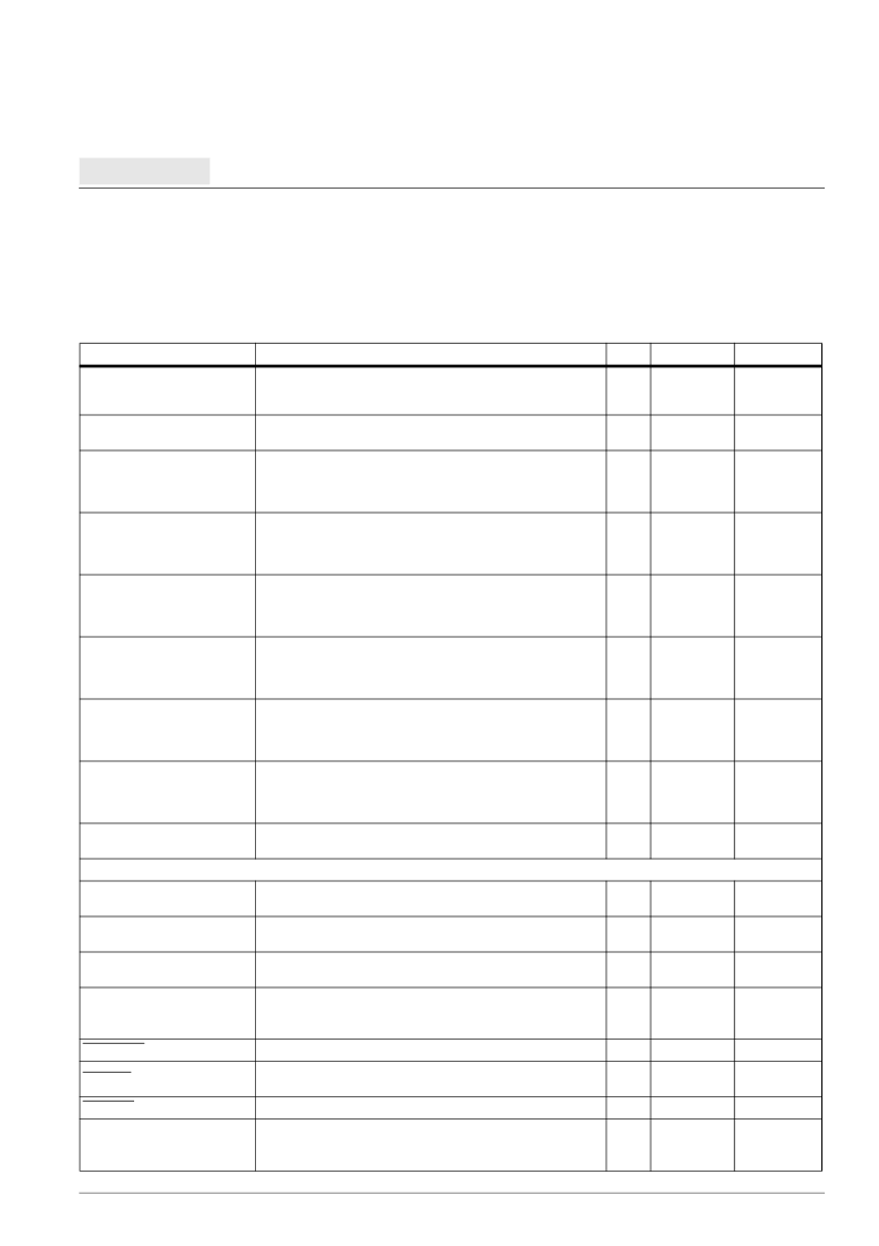
GMCCrS,
GMC1TxClk,
RTBI1TxClk
GMII: Carrier sense
RGMII: Transmit clock
RTBI: Transmit clock
I/O
3.3V tolerant
2.5V CMOS
GMCRefClk
GMII, RGMII, TBI and RTBI: Gigabit reference clock
I
3.3V tolerant
2.5V CMOS
5
GMCRxD0:3,
GMC0RxD0:3,
TBIRxD0:3,
RTBI0RxD0:3
GMII: Receive data
RGMII: Receive data
TBI: Receive data
RTBI: Receive data
I
3.3V tolerant
2.5V CMOS
GMCRxD4:7,
GMC1RxD0:3,
TBIRxD4:7,
RTBI1RxD0:3
GMII: Receive data
RGMII: Receive data
TBI: Receive data
RTBI: Receive data
I
3.3V tolerant
2.5V CMOS
GMCRxDV,
GMC0RxCtl,
TBIRxD8,
RTBI0RxD4
GMII: Receive data valid
RGMII: Receive control
TBI: Receive data
RTBI: Receive data
I
3.3V tolerant
2.5V CMOS
GMCRxEr,
GMC1RxCtl,
TBIRxD9,
RTBI1RxD4
GMII: Receive error
RGMII: Receive control
TBI: Receive data
RTBI: Receive data
I/O
3.3V tolerant
2.5V CMOS
GMCTxEn,
GMC0TxCtl,
TBITxD8,
RTBI0TxD4
GMII: Transmit data enable
RGMII: Transmit control
TBI: Transmit data
RTBI: Transmit data
O
3.3V tolerant
2.5V CMOS
GMCTxEr,
GMC1TxCtl,
TBITxD9,
RTBI1TxD4
GMII: Transmit error
RGMII: Transmit control
TBI: Transmit data
RTBI: Transmit data
O
3.3V tolerant
2.5V CMOS
6
GMCTxClk
TBIRxClk1
GMII: 10/100Mbps Transmit clock
TBI: Receive clock 1
I/O
3.3V LVTTL
5
External Slave Peripheral Interface
DMAAck0:3
Used by the PPC440GX to indicate that data transfers have
occurred.
O
3.3V tolerant
2.5V CMOS
DMAReq0:3
Used by slave peripherals to indicate they are prepared to transfer
data.
I
3.3V tolerant
2.5V CMOS
1, 5
EOT0:3/TC0:3
End Of Transfer/Terminal Count.
I/O
3.3V tolerant
2.5V CMOS
1, 5
PerAddr00:31
Peripheral address bus used by PPC440GX when not in external
master mode, otherwise used by external master.
Note:
PerAddr00 is the most significant bit (msb) on this bus.
I/O
3.3V LVTTL
1
PerWBE0:3
External peripheral data bus byte enables.
I/O
3.3V LVTTL
1, 2
PerBLast
Used by either the peripheral controller, DMA controller, or
external master to indicates the last transfer of a memory access.
I/O
3.3V LVTTL
1, 4
PerCS0:7
External peripheral device select.
O
3.3V LVTTL
2
PerData00:31
Peripheral data bus used by PPC440GX when not in external
master mode, otherwise used by external master.
Note:
PerData00 is the most significant bit (msb) on this bus.
I/O
3.3V LVTTL
1
Signal Functional Description
(Sheet 4 of 8)
Notes:
1. Receiver input has hysteresis
2. Must pull up (recommended value is 3k
Ω
to 3.3V
)
3. Must pull down (recommended value is 1k
Ω
)
4. If not used, must pull up (recommended value is 3k
Ω
to 3.3V)
5. If not used, must pull down (recommended value is 1k
Ω
)
6. Strapping input during reset; pull-up or pull-down required
Signal Name
Description
I/O
Type
Notes
相關(guān)PDF資料 |
PDF描述 |
|---|---|
| PPC440GX-3CF533E | Power PC 440GX Embedded Processor |
| PPC440GX-3CF667C | Power PC 440GX Embedded Processor |
| PPC440GX-3CF667CZ | Power PC 440GX Embedded Processor |
| PPC440GX-3CF800C | Power PC 440GX Embedded Processor |
| PPC440GX-3CF800CZ | Power PC 440GX Embedded Processor |
相關(guān)代理商/技術(shù)參數(shù) |
參數(shù)描述 |
|---|---|
| PPC440GX-3CF533E | 制造商:AMCC 制造商全稱:Applied Micro Circuits Corporation 功能描述:Power PC 440GX Embedded Processor |
| PPC440GX-3CF667C | 制造商:AppliedMicro 功能描述:MPU 440GX RISC 32-Bit 0.13um 667MHz 3.3V 552-Pin CBGA Tray 制造商:AMCC 功能描述:MPU 440GX RISC 32BIT 0.13UM 667MHZ 3.3V 552CBGA - Trays 制造商:Applied Micro Circuits Corporation 功能描述:MPU 440GX RISC 32-Bit 0.13um 667MHz 3.3V 552-Pin CBGA Tray |
| PPC440GX-3CF667CZ | 制造商:AMCC 制造商全稱:Applied Micro Circuits Corporation 功能描述:Power PC 440GX Embedded Processor |
| PPC440GX-3CF800C | 制造商:AppliedMicro 功能描述:MPU 440GX RISC 32-Bit 0.13um 800MHz 3.3V 552-Pin CBGA Tray |
| PPC440GX-3CF800CZ | 制造商:AMCC 制造商全稱:Applied Micro Circuits Corporation 功能描述:Power PC 440GX Embedded Processor |
發(fā)布緊急采購,3分鐘左右您將得到回復(fù)。