- 您現(xiàn)在的位置:買賣IC網(wǎng) > PDF目錄378055 > PM7344 (PMC-SIERRA INC) SATURN QUAD T1/E1 MULTI-PHY USER NETWORK INTERFACE DEVICE PDF資料下載
參數(shù)資料
| 型號(hào): | PM7344 |
| 廠商: | PMC-SIERRA INC |
| 元件分類: | 通信及網(wǎng)絡(luò) |
| 英文描述: | SATURN QUAD T1/E1 MULTI-PHY USER NETWORK INTERFACE DEVICE |
| 中文描述: | SPECIALTY TELECOM CIRCUIT, PQFP128 |
| 封裝: | 14 X 20 MM, PLASTIC, QFP-128 |
| 文件頁數(shù): | 99/293頁 |
| 文件大小: | 1147K |
| 代理商: | PM7344 |
第1頁第2頁第3頁第4頁第5頁第6頁第7頁第8頁第9頁第10頁第11頁第12頁第13頁第14頁第15頁第16頁第17頁第18頁第19頁第20頁第21頁第22頁第23頁第24頁第25頁第26頁第27頁第28頁第29頁第30頁第31頁第32頁第33頁第34頁第35頁第36頁第37頁第38頁第39頁第40頁第41頁第42頁第43頁第44頁第45頁第46頁第47頁第48頁第49頁第50頁第51頁第52頁第53頁第54頁第55頁第56頁第57頁第58頁第59頁第60頁第61頁第62頁第63頁第64頁第65頁第66頁第67頁第68頁第69頁第70頁第71頁第72頁第73頁第74頁第75頁第76頁第77頁第78頁第79頁第80頁第81頁第82頁第83頁第84頁第85頁第86頁第87頁第88頁第89頁第90頁第91頁第92頁第93頁第94頁第95頁第96頁第97頁第98頁當(dāng)前第99頁第100頁第101頁第102頁第103頁第104頁第105頁第106頁第107頁第108頁第109頁第110頁第111頁第112頁第113頁第114頁第115頁第116頁第117頁第118頁第119頁第120頁第121頁第122頁第123頁第124頁第125頁第126頁第127頁第128頁第129頁第130頁第131頁第132頁第133頁第134頁第135頁第136頁第137頁第138頁第139頁第140頁第141頁第142頁第143頁第144頁第145頁第146頁第147頁第148頁第149頁第150頁第151頁第152頁第153頁第154頁第155頁第156頁第157頁第158頁第159頁第160頁第161頁第162頁第163頁第164頁第165頁第166頁第167頁第168頁第169頁第170頁第171頁第172頁第173頁第174頁第175頁第176頁第177頁第178頁第179頁第180頁第181頁第182頁第183頁第184頁第185頁第186頁第187頁第188頁第189頁第190頁第191頁第192頁第193頁第194頁第195頁第196頁第197頁第198頁第199頁第200頁第201頁第202頁第203頁第204頁第205頁第206頁第207頁第208頁第209頁第210頁第211頁第212頁第213頁第214頁第215頁第216頁第217頁第218頁第219頁第220頁第221頁第222頁第223頁第224頁第225頁第226頁第227頁第228頁第229頁第230頁第231頁第232頁第233頁第234頁第235頁第236頁第237頁第238頁第239頁第240頁第241頁第242頁第243頁第244頁第245頁第246頁第247頁第248頁第249頁第250頁第251頁第252頁第253頁第254頁第255頁第256頁第257頁第258頁第259頁第260頁第261頁第262頁第263頁第264頁第265頁第266頁第267頁第268頁第269頁第270頁第271頁第272頁第273頁第274頁第275頁第276頁第277頁第278頁第279頁第280頁第281頁第282頁第283頁第284頁第285頁第286頁第287頁第288頁第289頁第290頁第291頁第292頁第293頁
PM7344 S/UNI-MPH
DATA SHEET
PMC-950449
ISSUE 6
MULTI-PHY USER NETWORK INTERFACE
PROPRIETARY AND CONFIDENTIAL TO PMC-SIERRA, INC., AND FOR ITS CUSTOMERS’ INTERNAL USE
83
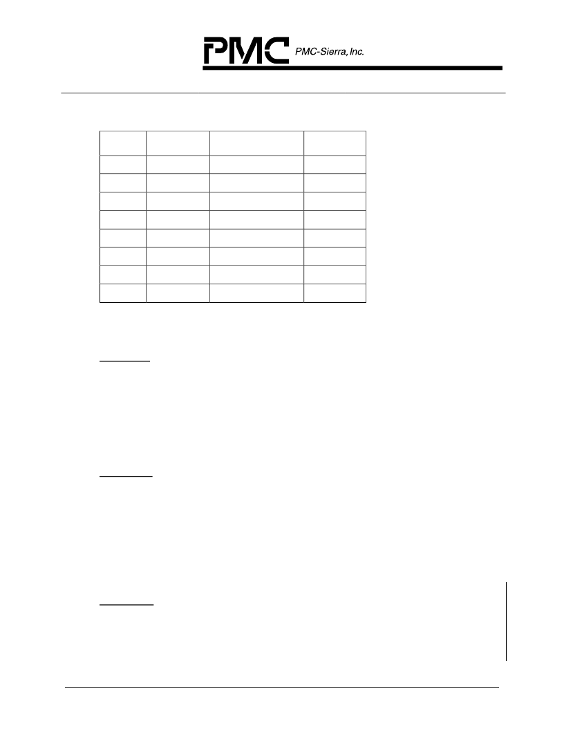
Registers 007H, 107H, 207H and 307H: Transmit Timing Options
Bit
Type
Function
Default
Bit 7
R/W
FIFOBYP
0
Bit 6
R/W
XCLKSEL
0
Bit 5
Unused
0
Bit 4
R/W
OCLKSEL
0
Bit 3
R/W
TREF[1]
0
Bit 2
R/W
TREF[0]
0
Bit 1
Unused
X
Bit 0
Unused
X
When the T1 or E1 format is selected, these registers allow software to configure
the options of the transmit timing section.
FIFOBYP:
The FIFOBYP bit enables the transmit input signals to DJAT to be bypassed
around the FIFO to the outputs. When jitter attenuation is not being used,
the DJAT FIFO can be bypassed to reduce the delay through the transmitter
section by typically 24 bits. When FIFOBYP is set to logic 1, the inputs to
DJAT are routed around the FIFO to the outputs. When FIFOBYP is set to
logic 0, the transmit data passes through the DJAT FIFO. When the T1 or E1
format is not enabled, the FIFO is automatically bypassed.
XCLKSEL:
The XCLKSEL bit selects the source of the high-speed clock used in the
CDRC and FRMR blocks. When XCLKSEL is set to logic 1, the XCLK input
signal is used as the high-speed clock to these blocks. XCLK must be driven
with clock that is 8 times the nominal bit rate (12.352 MHz for T1 or 16.384
MHz for E1). When XCLKSEL is set to logic 0, the high-speed clock is driven
by XCLK divided by 3. XCLK must be driven with a clock that is 24 times the
nominal bit rate (37.056MHz for T1 or 49.152 MHz for E1). XCLK must be
set to logic 0 when jitter attenuation is enabled.
OCLKSEL:
The OCLKSEL bit selects the source of the Digital Jitter Attenuator FIFO
output clock signal. When OCLKSEL is set to logic 1, the DJAT FIFO output
clock is driven with the transmit reference clock as selected by the TREF[1:0]
inputs. In this mode the jitter attenuation is disabled and the input clock must
相關(guān)PDF資料 |
PDF描述 |
|---|---|
| PM7345 | SATURN User Network Interface for PDH Applications |
| PM7346 | SATURN QUAD USER NETWORK INTERFACE FOR J2, E3, T3 |
| PM7347 | SATURN USER NETWORK INTERFACE for J2/E3/T3 |
| PM7347-BI | SATURN USER NETWORK INTERFACE for J2/E3/T3 |
| PM73487-PI | 622 Mbps ATM Traffic Management Device |
相關(guān)代理商/技術(shù)參數(shù) |
參數(shù)描述 |
|---|---|
| PM7344-RI | 制造商:PMC-Sierra 功能描述:7344-RI |
| PM7345 | 制造商:PMC 制造商全稱:PMC 功能描述:SATURN User Network Interface for PDH Applications |
| PM7345RI | 制造商:PMC-Sierra 功能描述: |
發(fā)布緊急采購,3分鐘左右您將得到回復(fù)。