- 您現(xiàn)在的位置:買賣IC網(wǎng) > PDF目錄368026 > PIC18F458ESOSQTP (Microchip Technology Inc.) High Performance, 28/40-Pin Enhanced FLASH Microcontrollers with CAN PDF資料下載
參數(shù)資料
| 型號(hào): | PIC18F458ESOSQTP |
| 廠商: | Microchip Technology Inc. |
| 英文描述: | High Performance, 28/40-Pin Enhanced FLASH Microcontrollers with CAN |
| 中文描述: | 高性能,28/40-Pin增強(qiáng)型閃存微控制器和CAN |
| 文件頁數(shù): | 51/384頁 |
| 文件大?。?/td> | 3119K |
| 代理商: | PIC18F458ESOSQTP |
第1頁第2頁第3頁第4頁第5頁第6頁第7頁第8頁第9頁第10頁第11頁第12頁第13頁第14頁第15頁第16頁第17頁第18頁第19頁第20頁第21頁第22頁第23頁第24頁第25頁第26頁第27頁第28頁第29頁第30頁第31頁第32頁第33頁第34頁第35頁第36頁第37頁第38頁第39頁第40頁第41頁第42頁第43頁第44頁第45頁第46頁第47頁第48頁第49頁第50頁當(dāng)前第51頁第52頁第53頁第54頁第55頁第56頁第57頁第58頁第59頁第60頁第61頁第62頁第63頁第64頁第65頁第66頁第67頁第68頁第69頁第70頁第71頁第72頁第73頁第74頁第75頁第76頁第77頁第78頁第79頁第80頁第81頁第82頁第83頁第84頁第85頁第86頁第87頁第88頁第89頁第90頁第91頁第92頁第93頁第94頁第95頁第96頁第97頁第98頁第99頁第100頁第101頁第102頁第103頁第104頁第105頁第106頁第107頁第108頁第109頁第110頁第111頁第112頁第113頁第114頁第115頁第116頁第117頁第118頁第119頁第120頁第121頁第122頁第123頁第124頁第125頁第126頁第127頁第128頁第129頁第130頁第131頁第132頁第133頁第134頁第135頁第136頁第137頁第138頁第139頁第140頁第141頁第142頁第143頁第144頁第145頁第146頁第147頁第148頁第149頁第150頁第151頁第152頁第153頁第154頁第155頁第156頁第157頁第158頁第159頁第160頁第161頁第162頁第163頁第164頁第165頁第166頁第167頁第168頁第169頁第170頁第171頁第172頁第173頁第174頁第175頁第176頁第177頁第178頁第179頁第180頁第181頁第182頁第183頁第184頁第185頁第186頁第187頁第188頁第189頁第190頁第191頁第192頁第193頁第194頁第195頁第196頁第197頁第198頁第199頁第200頁第201頁第202頁第203頁第204頁第205頁第206頁第207頁第208頁第209頁第210頁第211頁第212頁第213頁第214頁第215頁第216頁第217頁第218頁第219頁第220頁第221頁第222頁第223頁第224頁第225頁第226頁第227頁第228頁第229頁第230頁第231頁第232頁第233頁第234頁第235頁第236頁第237頁第238頁第239頁第240頁第241頁第242頁第243頁第244頁第245頁第246頁第247頁第248頁第249頁第250頁第251頁第252頁第253頁第254頁第255頁第256頁第257頁第258頁第259頁第260頁第261頁第262頁第263頁第264頁第265頁第266頁第267頁第268頁第269頁第270頁第271頁第272頁第273頁第274頁第275頁第276頁第277頁第278頁第279頁第280頁第281頁第282頁第283頁第284頁第285頁第286頁第287頁第288頁第289頁第290頁第291頁第292頁第293頁第294頁第295頁第296頁第297頁第298頁第299頁第300頁第301頁第302頁第303頁第304頁第305頁第306頁第307頁第308頁第309頁第310頁第311頁第312頁第313頁第314頁第315頁第316頁第317頁第318頁第319頁第320頁第321頁第322頁第323頁第324頁第325頁第326頁第327頁第328頁第329頁第330頁第331頁第332頁第333頁第334頁第335頁第336頁第337頁第338頁第339頁第340頁第341頁第342頁第343頁第344頁第345頁第346頁第347頁第348頁第349頁第350頁第351頁第352頁第353頁第354頁第355頁第356頁第357頁第358頁第359頁第360頁第361頁第362頁第363頁第364頁第365頁第366頁第367頁第368頁第369頁第370頁第371頁第372頁第373頁第374頁第375頁第376頁第377頁第378頁第379頁第380頁第381頁第382頁第383頁第384頁
2002 Microchip Technology Inc.
Preliminary
DS41159B-page 49
PIC18FXX8
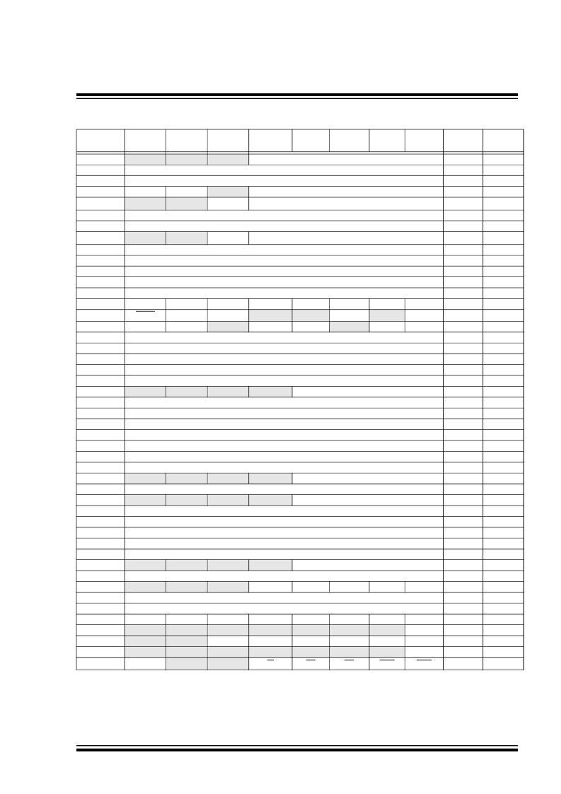
TABLE 4-2:
REGISTER FILE SUMMARY
File Name
Bit 7
Bit 6
Bit 5
Bit 4
Bit 3
Bit 2
Bit 1
Bit 0
Value on
POR, BOR
Details on
Page:
TOSU
TOSH
TOSL
STKPTR
—
—
—
Top-of-Stack Upper Byte (TOS<20:16>)
---0 0000
0000 0000
0000 0000
00-0 0000
30, 38
30, 38
30, 38
30, 39
Top-of-Stack High Byte (TOS<15:8>)
Top-of-Stack Low Byte (TOS<7:0>)
STKFUL
STKUNF
—
Return Stack Pointer
PCLATU
PCLATH
PCL
—
—
bit21
(2)
Holding Register for PC<20:16>
---0 0000
0000 0000
0000 0000
30, 40
30, 40
30, 40
Holding Register for PC<15:8>
PC Low Byte (PC<7:0>)
TBLPTRU
—
—
bit21
(2)
Program Memory Table Pointer Upper Byte (TBLPTR<20:16>)
--00 0000
0000 0000
0000 0000
0000 0000
xxxx xxxx
xxxx xxxx
0000 000x
30, 68
30, 68
30, 68
30, 68
30, 75
30, 75
30, 79
TBLPTRH
TBLPTRL
TABLAT
PRODH
PRODL
INTCON
Program Memory Table Pointer High Byte (TBLPTR<15:8>)
Program Memory Table Pointer Low Byte (TBLPTR<7:0>)
Program Memory Table Latch
Product Register High Byte
Product Register Low Byte
GIE/GIEH
PEIE/GIEL
TMR0IE
INT0IE
RBIE
TMR0IF
INT0IF
RBIF
INTCON2
INTCON3
INDF0
POSTINC0
POSTDEC0
PREINC0
PLUSW0
FSR0H
FSR0L
WREG
INDF1
POSTINC1
POSTDEC1
PREINC1
PLUSW1
FSR1H
FSR1L
BSR
INDF2
POSTINC2
POSTDEC2
PREINC2
PLUSW2
FSR2H
FSR2L
STATUS
TMR0H
TMR0L
T0CON
OSCCON
LVDCON
WDTCON
RBPU
INT2IP
Uses contents of FSR0 to address data memory - value of FSR0 not changed (not a physical register)
Uses contents of FSR0 to address data memory - value of FSR0 post-incremented (not a physical register)
Uses contents of FSR0 to address data memory - value of FSR0 post-incremented (not a physical register)
Uses contents of FSR0 to address data memory - value of FSR0 pre-incremented (not a physical register)
Uses contents of FSR0 to address data memory - value of FSR0 offset by W (not a physical register)
—
—
—
—
Indirect Data Memory Address Pointer 0 Low Byte
Working Register
Uses contents of FSR1 to address data memory - value of FSR1 not changed (not a physical register)
Uses contents of FSR1 to address data memory - value of FSR1 post-incremented (not a physical register)
Uses contents of FSR1 to address data memory - value of FSR1 post-incremented (not a physical register)
Uses contents of FSR1 to address data memory - value of FSR1 pre-incremented (not a physical register)
Uses contents of FSR1 to address data memory - value of FSR1 offset by W (not a physical register) -
—
—
—
—
Indirect Data Memory Address Pointer 1 Low Byte
—
—
—
—
Uses contents of FSR2 to address data memory - value of FSR2 not changed (not a physical register)
Uses contents of FSR2 to address data memory - value of FSR2 post-incremented (not a physical register)
Uses contents of FSR2 to address data memory - value of FSR2 post-incremented (not a physical register)
Uses contents of FSR2 to address data memory - value of FSR2 pre-incremented (not a physical register)
Uses contents of FSR2 to address data memory - value of FSR2 offset by W (not a physical register) -
—
—
—
—
Indirect Data Memory Address Pointer 2 Low Byte
—
—
—
N
Timer0 Register High Byte
Timer0 Register Low Byte
TMR0ON
T08BIT
T0CS
T0SE
—
—
—
—
—
—
IRVST
LVDEN
—
—
—
—
INTEDG0
INT1IP
INTEDG1
—
—
—
TMR0IP
—
—
RBIP
INT1IF
111- -1-1
11-1 0-00
n/a
n/a
n/a
n/a
n/a
---- xxxx
xxxx xxxx
uuuu uuuu
n/a
n/a
n/a
n/a
n/a
---- xxxx
xxxx xxxx
---- 0000
n/a
n/a
n/a
n/a
n/a
---- xxxx
xxxx xxxx
---x xxxx
0000 0000
xxxx xxxx
1111 1111
---- ---0
--00 0101
30, 80
30, 81
30, 55
30, 55
30, 55
30, 55
30, 55
30, 55
30, 55
30, 55
30, 55
30, 55
30, 55
30, 55
30, 55
31, 55
31, 55
31, 54
31, 55
31, 55
31, 55
31, 55
31, 55
31, 55
31, 55
31, 57
31, 109
31, 109
31, 107
31, 20
31, 257
31, 268
INT2IE
INT1IE
INT2IF
Indirect Data Memory Address Pointer 0 High
Indirect Data Memory Address Pointer 1 High
Bank Select Register
Indirect Data Memory Address Pointer 2 High
OV
Z
DC
C
PSA
—
LVDL3
—
T0PS2
—
LVDL2
—
T0PS1
—
LVDL1
—
T0PS0
SCS
LVDL0
SWDTEN
---- ---0
RCON
Legend:
Note
IPEN
—
—
RI
TO
PD
POR
BOR
0--1 11qq
31, 58, 91
x
= unknown,
u
= unchanged, - = unimplemented,
q
= value depends on condition
These registers or register bits are not implemented on the PIC18F248 and PIC18F258 and read as
’
0
’
s.
Bit21 of the TBLPTRU allows access to the device configuration bits.
RA6 and associated bits are configured as port pins in RCIO and ECIO Oscillator mode only and read
‘
0
’
in all other Oscillator
modes.
1:
2:
3:
相關(guān)PDF資料 |
PDF描述 |
|---|---|
| PIC18F458ESPQTP | High Performance, 28/40-Pin Enhanced FLASH Microcontrollers with CAN |
| PIC18F458ESPSQTP | High Performance, 28/40-Pin Enhanced FLASH Microcontrollers with CAN |
| PIC18F458ILQTP | High Performance, 28/40-Pin Enhanced FLASH Microcontrollers with CAN |
| PIC18F458ILSQTP | High Performance, 28/40-Pin Enhanced FLASH Microcontrollers with CAN |
| PIC18F458IPQTP | High Performance, 28/40-Pin Enhanced FLASH Microcontrollers with CAN |
相關(guān)代理商/技術(shù)參數(shù) |
參數(shù)描述 |
|---|---|
| PIC18F458-I/L | 功能描述:8位微控制器 -MCU 32KB 1536 RAM 34 I/O RoHS:否 制造商:Silicon Labs 核心:8051 處理器系列:C8051F39x 數(shù)據(jù)總線寬度:8 bit 最大時(shí)鐘頻率:50 MHz 程序存儲(chǔ)器大小:16 KB 數(shù)據(jù) RAM 大小:1 KB 片上 ADC:Yes 工作電源電壓:1.8 V to 3.6 V 工作溫度范圍:- 40 C to + 105 C 封裝 / 箱體:QFN-20 安裝風(fēng)格:SMD/SMT |
| PIC18F458-I/L | 制造商:Microchip Technology Inc 功能描述:IC 8BIT FLASH MCU CAN ADC 18F458 |
| PIC18F458-I/P | 功能描述:8位微控制器 -MCU 32KB 1536 RAM 34 I/O RoHS:否 制造商:Silicon Labs 核心:8051 處理器系列:C8051F39x 數(shù)據(jù)總線寬度:8 bit 最大時(shí)鐘頻率:50 MHz 程序存儲(chǔ)器大小:16 KB 數(shù)據(jù) RAM 大小:1 KB 片上 ADC:Yes 工作電源電壓:1.8 V to 3.6 V 工作溫度范圍:- 40 C to + 105 C 封裝 / 箱體:QFN-20 安裝風(fēng)格:SMD/SMT |
| PIC18F458-I/P | 制造商:Microchip Technology Inc 功能描述:IC 8BIT FLASH MCU CAN ADC 18F458 |
| PIC18F458-I/PT | 功能描述:8位微控制器 -MCU 32KB 1536 RAM 34 I/O RoHS:否 制造商:Silicon Labs 核心:8051 處理器系列:C8051F39x 數(shù)據(jù)總線寬度:8 bit 最大時(shí)鐘頻率:50 MHz 程序存儲(chǔ)器大小:16 KB 數(shù)據(jù) RAM 大小:1 KB 片上 ADC:Yes 工作電源電壓:1.8 V to 3.6 V 工作溫度范圍:- 40 C to + 105 C 封裝 / 箱體:QFN-20 安裝風(fēng)格:SMD/SMT |
發(fā)布緊急采購,3分鐘左右您將得到回復(fù)。