- 您現(xiàn)在的位置:買賣IC網(wǎng) > PDF目錄368024 > pic16ce624 (Microchip Technology Inc.) OTP 8-Bit CMOS MCU with EEPROM Data Memory(8位OTP CMOS微控制器) PDF資料下載
參數(shù)資料
| 型號: | pic16ce624 |
| 廠商: | Microchip Technology Inc. |
| 英文描述: | OTP 8-Bit CMOS MCU with EEPROM Data Memory(8位OTP CMOS微控制器) |
| 中文描述: | 檢察官辦公室8位CMOS微控制器EEPROM數(shù)據(jù)存儲器(8位檢察官辦公室的CMOS微控制器) |
| 文件頁數(shù): | 10/108頁 |
| 文件大?。?/td> | 2355K |
| 代理商: | PIC16CE624 |
第1頁第2頁第3頁第4頁第5頁第6頁第7頁第8頁第9頁當(dāng)前第10頁第11頁第12頁第13頁第14頁第15頁第16頁第17頁第18頁第19頁第20頁第21頁第22頁第23頁第24頁第25頁第26頁第27頁第28頁第29頁第30頁第31頁第32頁第33頁第34頁第35頁第36頁第37頁第38頁第39頁第40頁第41頁第42頁第43頁第44頁第45頁第46頁第47頁第48頁第49頁第50頁第51頁第52頁第53頁第54頁第55頁第56頁第57頁第58頁第59頁第60頁第61頁第62頁第63頁第64頁第65頁第66頁第67頁第68頁第69頁第70頁第71頁第72頁第73頁第74頁第75頁第76頁第77頁第78頁第79頁第80頁第81頁第82頁第83頁第84頁第85頁第86頁第87頁第88頁第89頁第90頁第91頁第92頁第93頁第94頁第95頁第96頁第97頁第98頁第99頁第100頁第101頁第102頁第103頁第104頁第105頁第106頁第107頁第108頁
PIC16CE62X
DS40182A-page 10
Preliminary
1998 Microchip Technology Inc.
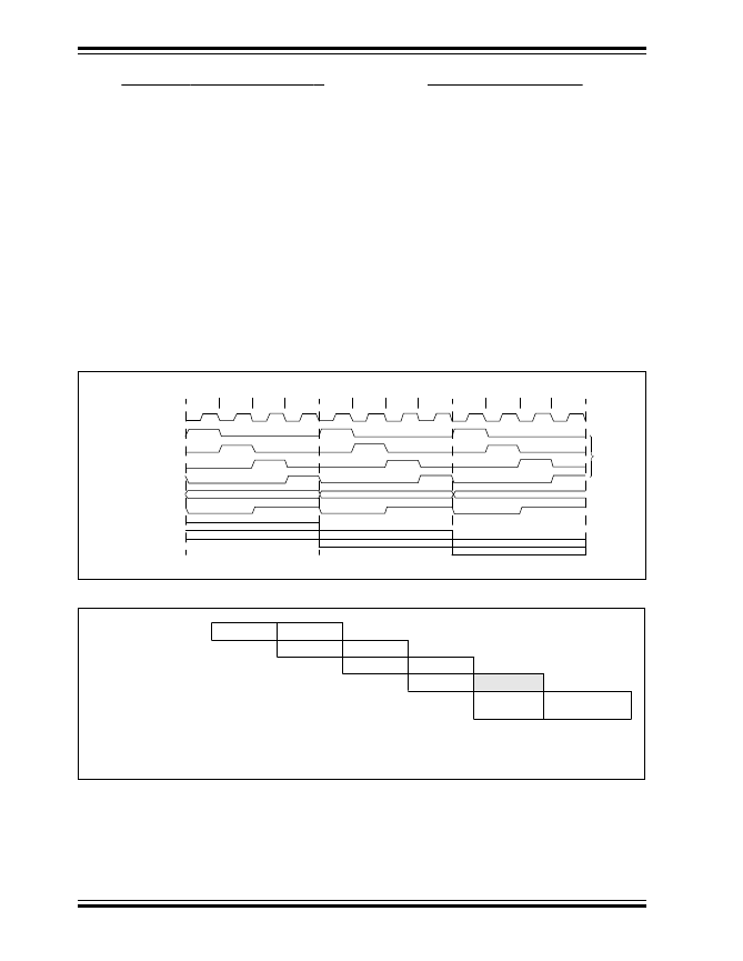
3.1
Clocking Scheme/Instruction Cycle
The clock input (OSC1/CLKIN pin) is internally divided
by four to generate four non-overlapping quadrature
clocks namely Q1, Q2, Q3 and Q4. Internally, the
program counter (PC) is incremented every Q1, the
instruction is fetched from the program memory and
latched into the instruction register in Q4. The
instruction is decoded and executed during the
following Q1 through Q4. The clocks and instruction
execution flow is shown in Figure 3-2.
3.2
Instruction Flow/Pipelining
An “Instruction Cycle” consists of four Q cycles (Q1,
Q2, Q3 and Q4). The instruction fetch and execute are
pipelined such that fetch takes one instruction cycle
while decode and execute takes another instruction
cycle. However, due to the pipelining, each instruction
effectively executes in one cycle. If an instruction
causes the program counter to change (e.g.,
GOTO
then two cycles are required to complete the instruction
(Example 3-1).
A fetch cycle begins with the program counter (PC)
incrementing in Q1.
In the execution cycle, the fetched instruction is latched
into the “Instruction Register (IR)” in cycle Q1. This
instruction is then decoded and executed during the
Q2, Q3, and Q4 cycles. Data memory is read during Q2
(operand read) and written during Q4 (destination
write).
)
FIGURE 3-2:
CLOCK/INSTRUCTION CYCLE
EXAMPLE 3-1:
INSTRUCTION PIPELINE FLOW
Q1
Q2
Q3
Q4
Q1
Q2
Q3
Q4
Q1
Q2
Q3
Q4
OSC1
Q1
Q2
Q3
Q4
PC
OSC(RC mode)
PC
PC+1
PC+2
Fetch INST (PC)
Execute INST (PC-1)
Fetch INST (PC+1)
Execute INST (PC)
Fetch INST (PC+2)
Internal
All instructions are single cycle, except for any program branches. These take two cycles since the fetch
instruction is “flushed” from the pipeline while the new instruction is being fetched and then executed.
1. MOVLW 55h
Fetch 1
Execute 1
Fetch 2
2. MOVWF PORTB
Execute 2
Fetch 3
3. CALL SUB_1
Execute 3
Fetch 4
4. BSF PORTA, BIT3
Flush
5. Instruction @
address SUB_1
Fetch SUB_1 Execute SUB_1
相關(guān)PDF資料 |
PDF描述 |
|---|---|
| pic16ce625 | OTP 8-Bit CMOS MCU with EEPROM Data Memory(8位OTP CMOS微控制器) |
| pic16cr54c | ROM-Based 8-Bit CMOS Microcontroller Series(8位CMOS微控制器) |
| PIC16CR73 | 28/40-Pin, 8-Bit CMOS ROM Microcontrollers |
| PIC16CR74 | 28/40-Pin, 8-Bit CMOS ROM Microcontrollers |
| PIC16CR76 | 28/40-Pin, 8-Bit CMOS ROM Microcontrollers |
相關(guān)代理商/技術(shù)參數(shù) |
參數(shù)描述 |
|---|---|
| PIC16CE624/JW | 功能描述:8位微控制器 -MCU 1.75KB 96 RAM 13 I/O RoHS:否 制造商:Silicon Labs 核心:8051 處理器系列:C8051F39x 數(shù)據(jù)總線寬度:8 bit 最大時鐘頻率:50 MHz 程序存儲器大小:16 KB 數(shù)據(jù) RAM 大小:1 KB 片上 ADC:Yes 工作電源電壓:1.8 V to 3.6 V 工作溫度范圍:- 40 C to + 105 C 封裝 / 箱體:QFN-20 安裝風(fēng)格:SMD/SMT |
| PIC16CE624-04/P | 功能描述:8位微控制器 -MCU 1.75KB 96 RAM 13 I/O RoHS:否 制造商:Silicon Labs 核心:8051 處理器系列:C8051F39x 數(shù)據(jù)總線寬度:8 bit 最大時鐘頻率:50 MHz 程序存儲器大小:16 KB 數(shù)據(jù) RAM 大小:1 KB 片上 ADC:Yes 工作電源電壓:1.8 V to 3.6 V 工作溫度范圍:- 40 C to + 105 C 封裝 / 箱體:QFN-20 安裝風(fēng)格:SMD/SMT |
| PIC16CE624-04/P | 制造商:Microchip Technology Inc 功能描述:IC 8BIT CMOS MCU 16CE624 DIP18 |
| PIC16CE624-04/SO | 功能描述:8位微控制器 -MCU 1.75KB 96 RAM 13 I/O RoHS:否 制造商:Silicon Labs 核心:8051 處理器系列:C8051F39x 數(shù)據(jù)總線寬度:8 bit 最大時鐘頻率:50 MHz 程序存儲器大小:16 KB 數(shù)據(jù) RAM 大小:1 KB 片上 ADC:Yes 工作電源電壓:1.8 V to 3.6 V 工作溫度范圍:- 40 C to + 105 C 封裝 / 箱體:QFN-20 安裝風(fēng)格:SMD/SMT |
| PIC16CE624-04/SS | 功能描述:8位微控制器 -MCU 1.75KB 96 RAM 13 I/O RoHS:否 制造商:Silicon Labs 核心:8051 處理器系列:C8051F39x 數(shù)據(jù)總線寬度:8 bit 最大時鐘頻率:50 MHz 程序存儲器大小:16 KB 數(shù)據(jù) RAM 大小:1 KB 片上 ADC:Yes 工作電源電壓:1.8 V to 3.6 V 工作溫度范圍:- 40 C to + 105 C 封裝 / 箱體:QFN-20 安裝風(fēng)格:SMD/SMT |
發(fā)布緊急采購,3分鐘左右您將得到回復(fù)。