- 您現(xiàn)在的位置:買賣IC網(wǎng) > PDF目錄367723 > P87C550EFAA (NXP SEMICONDUCTORS) AT25F1024 1M BIT SPI FLASH - SO8 PDF資料下載
參數(shù)資料
| 型號(hào): | P87C550EFAA |
| 廠商: | NXP SEMICONDUCTORS |
| 元件分類: | 微控制器/微處理器 |
| 英文描述: | AT25F1024 1M BIT SPI FLASH - SO8 |
| 中文描述: | 8-BIT, OTPROM, 8 MHz, MICROCONTROLLER, PQCC44 |
| 封裝: | PLASTIC, LCC-44 |
| 文件頁數(shù): | 5/28頁 |
| 文件大小: | 190K |
| 代理商: | P87C550EFAA |
第1頁第2頁第3頁第4頁當(dāng)前第5頁第6頁第7頁第8頁第9頁第10頁第11頁第12頁第13頁第14頁第15頁第16頁第17頁第18頁第19頁第20頁第21頁第22頁第23頁第24頁第25頁第26頁第27頁第28頁
Philips Semiconductors
Product specification
80C550/83C550/87C550
80C51 8-bit microcontroller family
4K/128 OTP/ROM/ROMless, 8 channel 8 bit A/D, watchdog timer
1998 May 01
5
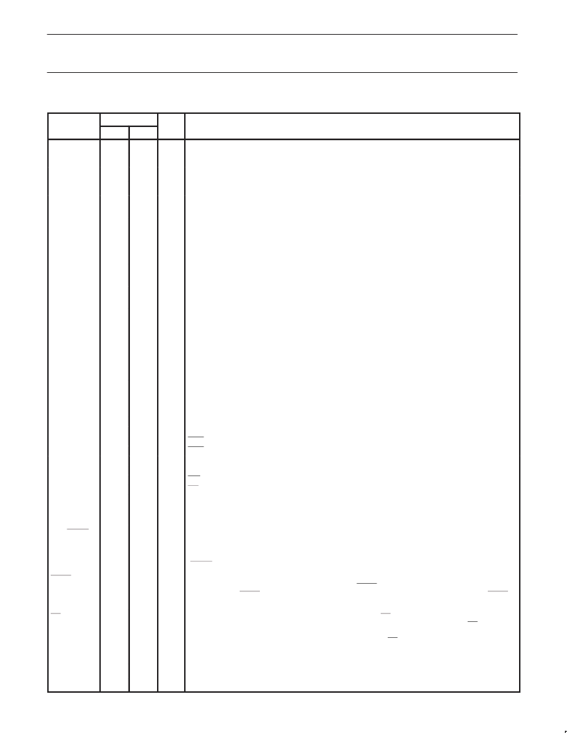
PIN DESCRIPTION
PIN NO.
MNEMONIC
DIP
LCC
TYPE
NAME AND FUNCTION
V
SS
20
24
I
Ground:
0V reference.
V
CC
40
44
I
Power Supply:
This is the power supply voltage for normal, idle, and power-down operation.
AV
CC
1
1
I
Analog Power Supply:
Analog supply voltage.
AV
SS
2
4
I
Analog Ground:
Analog 0V reference.
Vref+
Vref–
2
3
I
I
Vref:
A/D converter reference level inputs. Note that these references are combined with AV
CC
and
AV
SS
in the 40-pin DIP package.
P0.0–0.7
39–32
43–36
I/O
Port 0:
Port 0 is an open-drain, bidirectional I/O port. Port 0 pins that have 1s written to them float
and can be used as high-impedance inputs. Port 0 is also the multiplexed low-order address and
data bus during accesses to external program and data memory. In this application, it uses strong
internal pull-ups when emitting 1s. Port 0 also outputs the code bytes during program verification in
the S87C550. External pull-ups are required during program verification.
P1.0–P1.7
3–8
5–12
I
Port 1:
Port 1 is an 8-bit input only port (6-bit in the DIP package; bits P1.6 and P1.7 are not
implemented). Port 1 digital input can be read out any time.
ADC0–ADC7
3–8
5–12
ADCx:
Inputs to the analog multiplexer input of the 8-bit A/D. There are only six A/D inputs in the
DIP package.
P2.0–P2.7
21–28
25–32
I/O
Port 2:
Port 2 is an 8-bit bidirectional I/O port with internal pull-ups. Port 2 pins that have 1s written
to them are pulled high by the internal pull-ups and can be used as inputs. As inputs, port 2 pins that
are externally being pulled low will source current because of the internal pull-ups. (See DC
Electrical Characteristics: I
). Port 2 emits the high-order address byte during fetches from external
program memory and during accesses to external data memory that use 16-bit addresses (MOVX
@DPTR). In this application, it uses strong internal pull-ups when emitting 1s. During accesses to
external data memory that use 8-bit addresses (MOV @Ri), port 2 emits the contents of the P2
special function register.
P3.0–P3.7
10–17
14–21
I/O
Port 3:
Port 3 is an 8-bit bidirectional I/O port with internal pull-ups. Port 3 pins that have 1s written
to them are pulled high by the internal pull-ups and can be used as inputs. As inputs, port 3 pins that
are externally being pulled low will source current because of the pull-ups. (See DC Electrical
Characteristics: I
IL
). Port 3 also serves the special features of the SC80C51 family, as listed below:
RxD (P3.0):
Serial input port
TxD (P3.1):
Serial output port
INT0 (P3.2):
External interrupt
INT1 (P3.3):
External interrupt
T0 (P3.4):
Timer 0 external input
T1 (P3.5):
Timer 1 external input
WR (P3.6):
External data memory write strobe
RD (P3.7):
External data memory read strobe
10
11
12
13
14
15
16
17
14
15
16
17
18
19
20
21
I
O
I
I
I
I
O
O
RST
9
13
I
Reset:
A high on this pin for two machine cycles while the oscillator is running, resets the device.
An internal diffused resistor to V
SS
permits a power-on reset using only an external capacitor to
V
CC
.
ALE/PROG
30
34
I/O
Address Latch Enable/Program Pulse:
Output pulse for latching the low byte of the address
during an access to external memory. In normal operation, ALE is emitted at a constant rate of 1/6
the oscillator frequency, and can be used for external timing or clocking. Note that one ALE pulse is
skipped during each access to external data memory. This pin is also the program pulse input
(PROG) during EPROM programming.
PSEN
29
33
O
Program Store Enable:
The read strobe to external program memory. When the device is
executing code from the external program memory, PSEN is activated twice each machine cycle,
except that two PSEN activations are skipped during each access to external data memory. PSEN
is not activated during fetches from internal program memory.
EA/V
PP
31
35
I
External Access Enable/Programming Supply Voltage:
EA must be externally held low to enable
the device to fetch code from external program memory locations 0000H to 0FFFH. If EA is held
high, the device executes from internal program memory unless the program counter contains an
address greater than 0FFFH. For the 80C550 ROMless part, EA must be held low for the part to
operate properly. This pin also receives the 12.75V programming supply voltage (V
PP
) during
EPROM programming.
XTAL1
19
23
I
Crystal 1:
Input to the inverting oscillator amplifier and input to the internal clock generator circuits.
XTAL2
18
22
O
Crystal 2:
Output from the inverting oscillator amplifier.
相關(guān)PDF資料 |
PDF描述 |
|---|---|
| P80C557E4EBB | Single-chip 8-bit microcontroller |
| P80C557E8 | 8 BIT MICROCONTROLLER |
| P83C557E8 | 8 BIT MICROCONTROLLER |
| P83C557E4EBB | Single-chip 8-bit microcontroller |
| P83C557E4EFB | Single-chip 8-bit microcontroller |
相關(guān)代理商/技術(shù)參數(shù) |
參數(shù)描述 |
|---|---|
| P87C550EFAA-T | 制造商:未知廠家 制造商全稱:未知廠家 功能描述:8-Bit Microcontroller |
| P87C550EFFA | 制造商:未知廠家 制造商全稱:未知廠家 功能描述:8-Bit Microcontroller |
| P87C550EFK | 制造商:未知廠家 制造商全稱:未知廠家 功能描述:8-Bit Microcontroller |
| P87C550EFKA | 制造商:未知廠家 制造商全稱:未知廠家 功能描述:8-Bit Microcontroller |
| P87C550EFN | 制造商:未知廠家 制造商全稱:未知廠家 功能描述:8-Bit Microcontroller |
發(fā)布緊急采購,3分鐘左右您將得到回復(fù)。