- 您現(xiàn)在的位置:買賣IC網(wǎng) > PDF目錄367734 > P87C453EBAA (NXP SEMICONDUCTORS) 80C51 8-bit microcontroller family 8K/256 OTP/ROM, expanded I/O PDF資料下載
參數(shù)資料
| 型號: | P87C453EBAA |
| 廠商: | NXP SEMICONDUCTORS |
| 元件分類: | 微控制器/微處理器 |
| 英文描述: | 80C51 8-bit microcontroller family 8K/256 OTP/ROM, expanded I/O |
| 中文描述: | 8-BIT, OTPROM, 8 MHz, MICROCONTROLLER, PQCC68 |
| 封裝: | PLASTIC, SOT-168-3, MO-047AE, LCC-68 |
| 文件頁數(shù): | 14/26頁 |
| 文件大小: | 188K |
| 代理商: | P87C453EBAA |
第1頁第2頁第3頁第4頁第5頁第6頁第7頁第8頁第9頁第10頁第11頁第12頁第13頁當(dāng)前第14頁第15頁第16頁第17頁第18頁第19頁第20頁第21頁第22頁第23頁第24頁第25頁第26頁
Philips Semiconductors
Preliminary specification
83C453/87C453
80C51 8-bit microcontroller family
8K/256 OTP/ROM, expanded I/O
1998 Apr 23
14
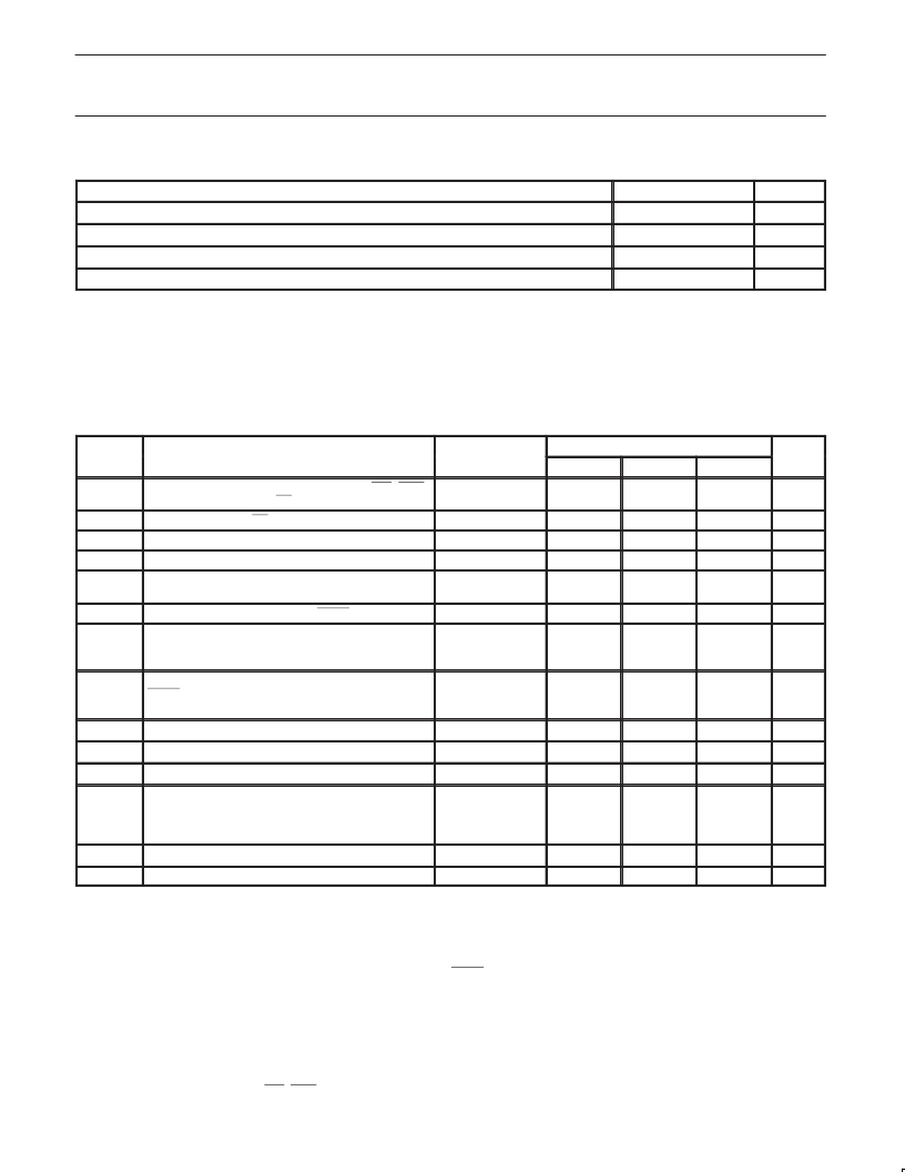
ABSOLUTE MAXIMUM RATINGS
1, 2, 3
PARAMETER
RATING
UNIT
Operating temperature under bias
0 to +70
°
C
Storage temperature range
–65 to +150
°
C
Voltage on any other pin to V
SS
–0.5 to +6.5
V
Power dissipation (based on package heat transfer limitations, not device power consumption)
1.5
W
NOTES:
1. Stresses above those listed under Absolute Maximum Ratings may cause permanent damage to the device. This is a stress rating only and
functional operation of the device at these or any conditions other than those described in the AC and DC Electrical Characteristics section
of this specification is not implied.
2. This product includes circuitry specifically designed for the protection of its internal devices from the damaging effects of excessive static
charge. Nonetheless, it is suggested that conventional precautions be taken to avoid applying greater than the rated maxima.
3. Parameters are valid over operating temperature range unless otherwise specified. Voltages are with respect to V
SS
unless otherwise noted.
DC ELECTRICAL CHARACTERISTICS
T
amb
= 0
°
C to +70
°
C, V
CC
= 5V
±
10%, V
SS
= 0V
TEST
LIMITS
TYP
1
SYMBOL
PARAMETER
CONDITIONS
MIN
MAX
UNIT
V
IL
Input low voltage; ports 0, 1, 2, 3, 4, 5, 6, IDS, ODS,
AFLAG, BFLAG; except EA
Input low voltage to EA
–0.5
0.2V
CC
–0.1
V
V
IL1
V
IH
V
IH1
V
OL
0
0.2V
CC
–0.3
V
CC
+0.5
V
CC
+0.5
0.45
V
Input high voltage; except XTAL1, RST
0.2V
CC
+0.9
0.7V
CC
V
Input high voltage; XTAL1, RST
V
Output low voltage; ports 1, 2, 3, 4, 5, 6, AFLAG,
BFLAG
Output low voltage; port 0, ALE, PSEN
I
OL
= 1.6mA
2
V
V
OL1
V
OH
I
OL
= 3.2mA
2
I
OH
= –60
μ
A,
I
OH
= –25
μ
A
I
OH
= –10
μ
A
I
OH
= –800
μ
A,
I
OH
= –300
μ
A
I
OH
= –80
μ
A
0.45
V
Output high voltage; ports 1, 2, 3, 4, 5, 6, AFLAG,
BFLAG
2.4
0.75V
CC
0.9V
CC
2.4
0.75V
CC
0.9V
CC
V
V
V
V
OH1
Output high voltage (port 0 in external bus mode, ALE,
PSEN)
3
V
V
V
I
IL
I
TL
Logical 0 input current,; ports 1, 2, 3, 4, 5, 6
V
IN
= 0.45V
See note 4
–50
μ
A
Logical 1-to-0 transition current; ports 1, 2, 3, 4, 5, 6
–650
μ
A
I
LI
I
CC
Input leakage current; port 0
V
IN
= V
IL
or V
IH
See note 6
±
10
μ
A
Power supply current:
Active mode @ 16MHz
5
Idle mode @ 16MHz
5
Power down mode
11.5
1.3
3
25
4
50
mA
mA
μ
A
k
R
RST
Internal reset pull-down resistor
50
300
C
IO
NOTES:
1. Typical ratings are based on a limited number of samples from early manufacturing lots, and not guaranteed. Values are room temp., 5V.
2. Capacitive loading on ports 0 and 2 may cause spurious noise to be superimposed on the V
OL
s of ALE and the other ports. The noise is due
to external bus capacitance discharging into the port 0 and port 2 pins when these pins make 1-to-0 transitions during bus operations. In the
worst cases (capacitive loading > 100pF), the noise pulse on the ALE pin may exceed 0.8V. In such cases, it may be desirable to qualify
ALE with a Schmitt Trigger, or use an address latch with a Schmitt Trigger STROBE input..
3. Capacitive loading on ports 0 and 2 may cause the V
OH
on ALE and PSEN to momentarily fall below the 0.9V
CC
specification when the
address bits are stabilizing.
4. Pins of ports 1, 2, 3, 4, 5 and 6 source a transition current when they are being externally driven from 1 to 0. The transition current reaches
its maximum value when V
IN
is approximately 2V.
5. I
CC
MAX at other frequencies is given by:
Active mode: I
CC
MAX = 0.94 X FREQ + 13.71
Idle mode: I
where FREQ is the external oscillator frequency in MHz. I
CC
MAX is given in mA. See Figure 20.
6. See Figures 21 through 24 for I
CC
test conditions.
7. C
IO
applies to ports 1 through 6, IDS, ODS, AFLAG, BFLAG, XTAL1, XTAL2.
Pin capacitance
7
– PLCC package
10
pF
相關(guān)PDF資料 |
PDF描述 |
|---|---|
| P83C453EBAA | 80C51 8-bit microcontroller family 8K/256 OTP/ROM, expanded I/O |
| P87C51MC2 | 80C51 8-bit microcontroller family with extended memory |
| P87C51MB2 | 80C51 8-bit microcontroller family with extended memory |
| P87C51RA2 | 80C51 8-bit microcontroller family |
| P87C51RA2BBD | Circular Connector; MIL SPEC:MIL-C-26482, Series I, Solder; Body Material:Aluminum; Series:PT06; No. of Contacts:18; Connector Shell Size:14; Connecting Termination:Solder; Circular Shell Style:Straight Plug; Gender:Female |
相關(guān)代理商/技術(shù)參數(shù) |
參數(shù)描述 |
|---|---|
| P87C453EBL | 制造商:未知廠家 制造商全稱:未知廠家 功能描述:8-Bit Microcontroller |
| P87C453EBLKA | 制造商:PHILIPS 制造商全稱:NXP Semiconductors 功能描述:CMOS single-chip 8-bit microcontrollers |
| P87C453EFAA | 制造商:PHILIPS 制造商全稱:NXP Semiconductors 功能描述:CMOS single-chip 8-bit microcontrollers |
| P87C453EFL | 制造商:未知廠家 制造商全稱:未知廠家 功能描述:8-Bit Microcontroller |
| P87C453EFLKA | 制造商:PHILIPS 制造商全稱:NXP Semiconductors 功能描述:CMOS single-chip 8-bit microcontrollers |
發(fā)布緊急采購,3分鐘左右您將得到回復(fù)。