- 您現(xiàn)在的位置:買賣IC網(wǎng) > PDF目錄367723 > P83C575EBBB (NXP SEMICONDUCTORS) 80C51 8-bit microcontroller family 8K/256 OTP/ROM/ROMless, 4 comparator, failure detect circuitry, watchdog timer PDF資料下載
參數(shù)資料
| 型號: | P83C575EBBB |
| 廠商: | NXP SEMICONDUCTORS |
| 元件分類: | 微控制器/微處理器 |
| 英文描述: | 80C51 8-bit microcontroller family 8K/256 OTP/ROM/ROMless, 4 comparator, failure detect circuitry, watchdog timer |
| 中文描述: | 8-BIT, MROM, 16 MHz, MICROCONTROLLER, PQFP44 |
| 封裝: | PLASTIC, SOT-307-2, QFP-44 |
| 文件頁數(shù): | 6/40頁 |
| 文件大?。?/td> | 383K |
| 代理商: | P83C575EBBB |
第1頁第2頁第3頁第4頁第5頁當前第6頁第7頁第8頁第9頁第10頁第11頁第12頁第13頁第14頁第15頁第16頁第17頁第18頁第19頁第20頁第21頁第22頁第23頁第24頁第25頁第26頁第27頁第28頁第29頁第30頁第31頁第32頁第33頁第34頁第35頁第36頁第37頁第38頁第39頁第40頁
Philips Semiconductors
Product specification
80C575/83C575/
87C575
80C51 8-bit microcontroller family
8K/256 OTP/ROM/ROMless, 4 comparator, failure detect circuitry, watchdog timer
1998 May 01
6
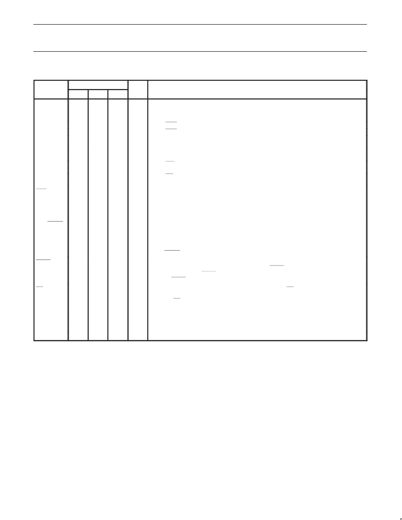
PIN DESCRIPTIONS
(Continued)
PIN NUMBER
MNEMONIC
DIP
LCC
QFP
TYPE
NAME AND FUNCTION
Port 3:
(continued)
P3.0
RxD
P3.1
TxD
P3.2
INT0
P3.3
INT1
P3.4
T0
CMPR-
P3.5
T1
CMP1+
P3.6
WR
CMP2+
P3.7
RD
CMP3+
10
11
12
13
14
11
13
14
15
16
5
7
8
9
10
I
Serial receive port
Serial transmit port enabled only when transmitting serial data
External interrupt 0
External interrupt 1
Timer/counter 0 input
Common - reference to comparators 1, 2, 3
Timer/counter 1 input
Comparator 1 positive input
External data memory write strobe
Comparator 2 positive input
External data memory read strobe
Comparator 3 positive input
O
I
I
I
15
17
11
I
16
18
12
O
17
19
13
O
RST
9
10
4
I
Reset:
A low on this pin asynchronously resets all port pins to a low state except P3.1. The
pin must be held low with the oscillator running for 24 oscillator cycles to initialize the
internal registers. An internal diffused resistor to V
permits a power on reset using only
an external capacitor to V
SS
. RST has a Schmitt trigger input stage to provide additional
noise immunity with a slow rising input voltage.
ALE/PROG
30
33
27
I/O
Address Latch Enable/Program Pulse:
Output pulse for latching the low byte of the
address during an access to external memory. In normal operation, ALE is emitted at a
constant rate of 1/6 the oscillator frequency, and can be used for external timing or clocking.
Note that one ALE pulse is skipped during each access to external data memory. ALE is
switched off if the bit 0 in the AUXR register (8EH) is set. This pin is also the program pulse
input (PROG) during EPROM programming.
PSEN
29
32
26
O
Program Store Enable:
The read strobe to external program memory. When the device is
executing code from the external program memory, PSEN is activated twice each machine
cycle, except that two PSEN activations are skipped during each access to external data
memory. PSEN is not activated during fetches from internal program memory.
EA/V
PP
31
35
29
I
External Access Enable/Programming Supply Voltage:
EA must be externally held low
to enable the device to fetch code from external program memory locations 0000H to
1FFFH. If EA is held high, the device executes from internal program memory unless the
program counter contains an address greater than 1FFFH. This pin also receives the
12.75V programming supply voltage (V
PP
) during EPROM programming.
Crystal 1:
Input to the inverting oscillator amplifier and input to the internal clock generator
circuits.
XTAL1
19
21
15
I
XTAL2
18
20
14
O
Crystal 2:
Output from the inverting oscillator amplifier.
相關(guān)PDF資料 |
PDF描述 |
|---|---|
| P87C575EBBB | 80C51 8-bit microcontroller family 8K/256 OTP/ROM/ROMless, 4 comparator, failure detect circuitry, watchdog timer |
| P80C591SFA | Single-chip 8-bit microcontroller with CAN controller |
| P83C591VFB | Single-chip 8-bit microcontroller with CAN controller |
| P87C591VFB | 27 PF 5% 50V NPO/COG (0805) CHIP CAP TR |
| P83C591SFA | Single-chip 8-bit microcontroller with CAN controller |
相關(guān)代理商/技術(shù)參數(shù) |
參數(shù)描述 |
|---|---|
| P83C575EBBB/CV5847 | 制造商:NXP Semiconductors 功能描述: |
| P83C575EBN | 制造商:未知廠家 制造商全稱:未知廠家 功能描述:Microcontroller |
| P83C575EBP | 制造商:未知廠家 制造商全稱:未知廠家 功能描述:8-Bit Microcontroller |
| P83C575EBPN | 制造商:PHILIPS 制造商全稱:NXP Semiconductors 功能描述:80C51 8-bit microcontroller family 8K/256 OTP/ROM/ROMless, 4 comparator, failure detect circuitry, watchdog timer |
| P83C575EFA | 制造商:未知廠家 制造商全稱:未知廠家 功能描述:8-Bit Microcontroller |
發(fā)布緊急采購,3分鐘左右您將得到回復(fù)。