- 您現(xiàn)在的位置:買(mǎi)賣(mài)IC網(wǎng) > PDF目錄369943 > P83C562EHA (NXP Semiconductors N.V.) 8-BIT MICROCONTROLLER PDF資料下載
參數(shù)資料
| 型號(hào): | P83C562EHA |
| 廠商: | NXP Semiconductors N.V. |
| 元件分類(lèi): | 8位微控制器 |
| 英文描述: | 8-BIT MICROCONTROLLER |
| 中文描述: | 8位微控制器 |
| 文件頁(yè)數(shù): | 30/52頁(yè) |
| 文件大小: | 299K |
| 代理商: | P83C562EHA |
第1頁(yè)第2頁(yè)第3頁(yè)第4頁(yè)第5頁(yè)第6頁(yè)第7頁(yè)第8頁(yè)第9頁(yè)第10頁(yè)第11頁(yè)第12頁(yè)第13頁(yè)第14頁(yè)第15頁(yè)第16頁(yè)第17頁(yè)第18頁(yè)第19頁(yè)第20頁(yè)第21頁(yè)第22頁(yè)第23頁(yè)第24頁(yè)第25頁(yè)第26頁(yè)第27頁(yè)第28頁(yè)第29頁(yè)當(dāng)前第30頁(yè)第31頁(yè)第32頁(yè)第33頁(yè)第34頁(yè)第35頁(yè)第36頁(yè)第37頁(yè)第38頁(yè)第39頁(yè)第40頁(yè)第41頁(yè)第42頁(yè)第43頁(yè)第44頁(yè)第45頁(yè)第46頁(yè)第47頁(yè)第48頁(yè)第49頁(yè)第50頁(yè)第51頁(yè)第52頁(yè)

1997 Apr 08
30
Philips Semiconductors
Product specification
8-bit microcontroller
P83C562; P80C562
16 OSCILLATOR CIRCUITRY
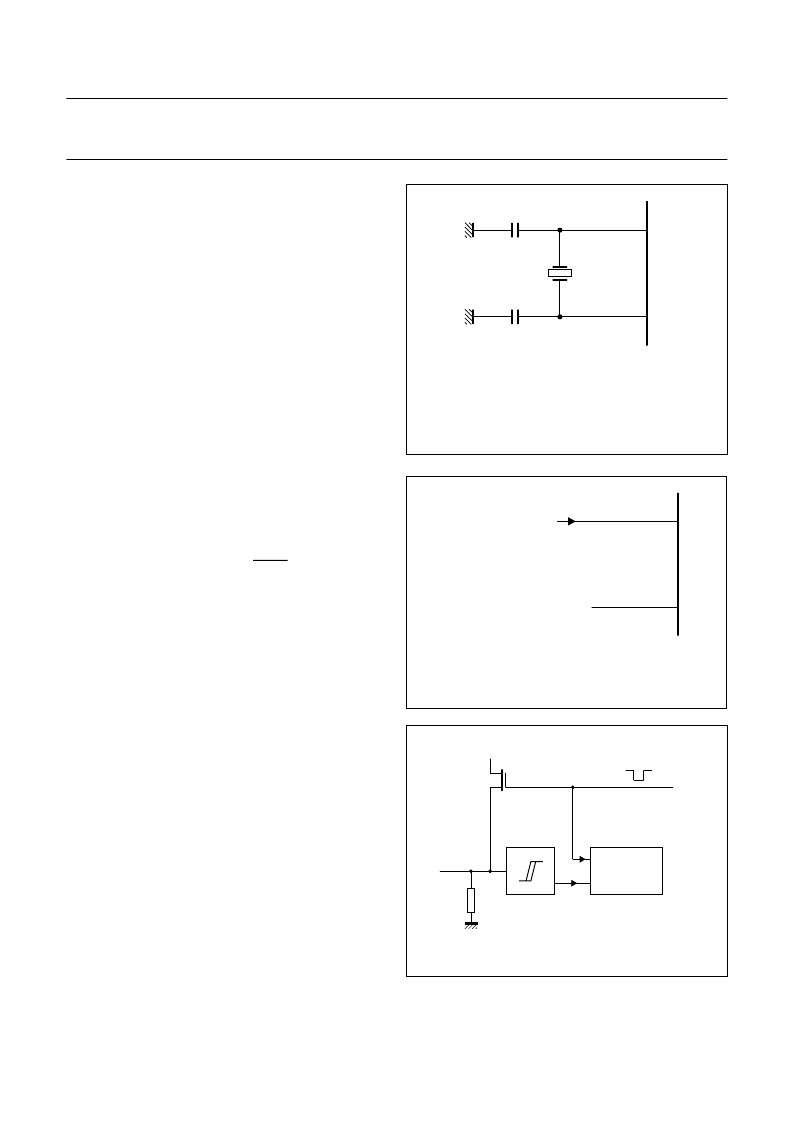
The oscillator circuitry of the P8xC562 is a single-stage
inverting amplifier in a Pierce oscillator configuration.
The circuitry between XTAL1 and XTAL2 is basically an
inverter biased to the transfer point. Either a crystal or
ceramic resonator can be used as the feedback element to
complete the oscillator circuitry. Both are operated in
parallel resonance. XTAL1 (pin 35) is the high gain
amplifier input, and XTAL2 (pin 34) is the output (see
Fig.14). To drive the P8xC562 externally, XTAL1 is driven
from an external source and XTAL2 left open-circuit (see
Fig.15).
17 RESET CIRCUITRY
The reset circuitry for the P8xC562 is connected to the
reset pin RST. A Schmitt trigger is used at the input for
noise rejection. The output of the Schmitt trigger is
sampled by the reset circuitry every machine cycle.
The on-chip Reset circuit is shown in Fig.16.
A reset is accomplished by holding the RST pin HIGH for
at least two machine cycles (24 oscillator periods but at
least 2
μ
s). The CPU responds by executing an internal
reset. During reset both ALE and PSEN output a HIGH
level. In order to perform a correct reset, this level must not
be affected by external elements.
Also with the P8xC562, the RST line can be pulled HIGH
internally by a pull-up transistor activated by the Watchdog
Timer (T3). The length of the output pulse from the
Watchdog Timer is 3 machine cycles. A pulse of such
short duration is necessary in order to recover from a
processor or system fault as fast as possible.
It can be seen that the short reset pulse from T3 cannot
discharge the Power-on reset capacitor (see Fig.17).
Consequently, when the Watchdog Timer is also used to
reset external devices this capacitor arrangement should
not be connected to the RST pin, and an extra circuit
should be used to perform the Power-on-reset operation.
It should be remembered that a T3 overflow, if enabled, will
force a reset condition to the P8xC562 by an internal
connection, whether the output RST is tied LOW or not.
The internal reset is executed during the second cycle in
which RST is HIGH and is repeated every cycle until RST
goes LOW. The internal RAM is not affected by reset.
When V
DD
is turned on, the RAM content is indeterminate.
An internal reset leaves the internal registers as shown in
Table 36.
Fig.14 P8xC562P8xC562 oscillator circuit.
1) Use fundamental crystals only.
k, halfpage
C1
XTAL1
XTAL2
20 pF
C2
MBC751
20 pF
35
34
(1)
Fig.15 Driving the P8xC562 from an external source.
ook, halfpage
XTAL1
XTAL2
MGA169
external clock
(not TTL
compatible)
not connected
35
34
Fig.16 On-chip reset configuration.
andbook, halfpage
MBC476 - 1
SCHMITT
TRIGGER
RESET
CIRCUITRY
overflow
timer T3
VDD
RST
on-chip
resistor
RST
R
發(fā)布緊急采購(gòu),3分鐘左右您將得到回復(fù)。