- 您現(xiàn)在的位置:買賣IC網(wǎng) > PDF目錄361102 > NCP5322ADWG (ON SEMICONDUCTOR) Two−Phase Buck Controller with Integrated Gate Drivers and 5−Bit DAC PDF資料下載
參數(shù)資料
| 型號(hào): | NCP5322ADWG |
| 廠商: | ON SEMICONDUCTOR |
| 元件分類: | 穩(wěn)壓器 |
| 英文描述: | Two−Phase Buck Controller with Integrated Gate Drivers and 5−Bit DAC |
| 中文描述: | 1.5 A SWITCHING CONTROLLER, 1000 kHz SWITCHING FREQ-MAX, PDSO28 |
| 封裝: | LEAD FREE, SOIC-28 |
| 文件頁(yè)數(shù): | 13/31頁(yè) |
| 文件大小: | 726K |
| 代理商: | NCP5322ADWG |
第1頁(yè)第2頁(yè)第3頁(yè)第4頁(yè)第5頁(yè)第6頁(yè)第7頁(yè)第8頁(yè)第9頁(yè)第10頁(yè)第11頁(yè)第12頁(yè)當(dāng)前第13頁(yè)第14頁(yè)第15頁(yè)第16頁(yè)第17頁(yè)第18頁(yè)第19頁(yè)第20頁(yè)第21頁(yè)第22頁(yè)第23頁(yè)第24頁(yè)第25頁(yè)第26頁(yè)第27頁(yè)第28頁(yè)第29頁(yè)第30頁(yè)第31頁(yè)
NCP5322A
http://onsemi.com
13
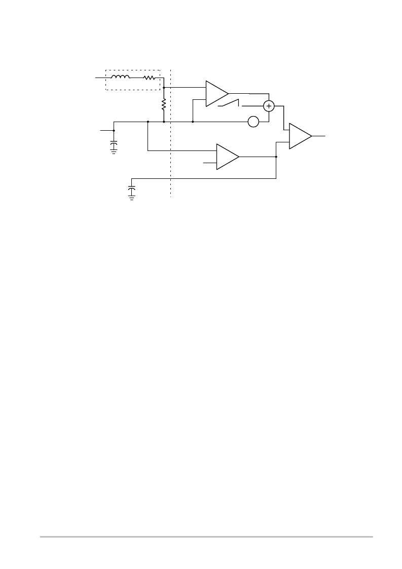
Figure 10. Enhanced V
2
Control Employing Resistive Current Sensing and Additional Internal Ramp
+
CSA
SWNODE
Ln
RLn
RSn
CSn
COn
CS
REF
+
V
OUT
(V
CORE
)
“FastFeedback”
Connection
+
PWM
COMP
To F/F
Reset
Channel
StartUp
Offset
+
E.A.
DAC
Out
V
FB
COMP
Internal Ramp
+
n = 1 or 2
+
Enhanced V
2
responds to disturbances in V
CORE
by
employing both “slow” and “fast” voltage regulation. The
internal error amplifier performs the slow regulation.
Depending on the gain and frequency compensation set by
the amplifier’s external components, the error amplifier will
typically begin to ramp its output to react to changes in the
output voltage in 12 PWM cycles. Fast voltage feedback is
implemented by a direct connection from V
CORE
to the
noninverting pin of the PWM comparator via the
summation with the inductor current, internal ramp, and
Offset. A rapid increase in load current will produce a
negative offset at V
CORE
and at the output of the summer.
This will cause the PWM duty cycle to increase almost
instantly. Fast feedback will typically adjust the PWM duty
cycle in 1 PWM cycle.
As shown in Figure 10, an internal ramp (nominally 125 mV
at a 50% duty cycle) is added to the inductor current ramp
at the positive terminal of the PWM comparator. This
additional ramp compensates for propagation time delays
from the current sense amplifier (CSA), the PWM
comparator, and the MOSFET gate drivers. As a result, the
minimum ON time of the controller is reduced and lower
duty cycles may be achieved at higher frequencies. Also, the
additional ramp reduces the reliance on the inductor current
ramp and allows greater flexibility when choosing the output
inductor and the R
CSn
C
CSn
(n = 1 or 2) time constant of the
feedback components from V
CORE
to the CSn pin.
Including both current and voltage information in the
feedback signal allows the open loop output impedance of
the power stage to be controlled. When the average output
current is zero, the COMP pin will be:
VCOMP
VOUT@ 0 A
Int_Ramp
Channel_Startup_Offset
GCSA
Ext_Ramp 2
Int_Ramp is the “partial” internal ramp value at the
corresponding duty cycle, Ext_Ramp is the peaktopeak
external steadystate ramp at 0 A, G
CSA
is the Current Sense
Amplifier Gain (nominally 3.5 V/V), and the Channel
Startup Offset is typically 0.40 V. The magnitude of the
Ext_Ramp can be calculated from:
Ext_Ramp
D
(VIN
VOUT) (RCSn
CCSn
fSW)
For example, if V
OUT
at 0 A is set to 1.630 V with AVP
and the input voltage is 12.0 V, the duty cycle (D) will be
1.630/12.0 or 13.6%. Int_Ramp will be 125 mV
13.6/50 =
34 mV. Realistic values for R
CSn
, C
CSn
and f
SW
are 60 k ,
0.01 F, and 220 kHz
using these and the previously
mentioned formula, Ext_Ramp will be 10.6 mV.
VCOMP
1.630 V
3.5 V V
2.083 Vdc.
0.40 V
10.6 mV 2
34 mV
If the COMP pin is held steady and the inductor current
changes, there must also be a change in the output voltage.
Or, in a closed loop configuration when the output current
changes, the COMP pin must move to keep the same output
voltage. The required change in the output voltage or COMP
pin depends on the scaling of the current feedback signal and
is calculated as:
V
RS
GCSA
IOUT.
The singlephase power stage output impedance is:
Single Stage Impedance
VOUT
IOUT
RS
GCSA
The multiphase power stage output impedance is the
singlephase output impedance divided by the number of
phases. The output impedance of the power stage determines
how the converter will respond during the first few
microseconds of a transient before the feedback loop has
repositioned the COMP pin.
The peak output current can be calculated from:
相關(guān)PDF資料 |
PDF描述 |
|---|---|
| NCP5322ADWR2G | Two−Phase Buck Controller with Integrated Gate Drivers and 5−Bit DAC |
| NCP5331FTR2G | Two-Phase PWM Controller with Integrated Gate Drivers |
| NCP5331 | Two-Phase PWM Controller with Integrated Gate Drivers |
| NCP5331FTR2 | Two-Phase PWM Controller with Integrated Gate Drivers |
| NCP5383 | Two Phase Buck Controller with Integrated Gate Drivers and AVP |
相關(guān)代理商/技術(shù)參數(shù) |
參數(shù)描述 |
|---|---|
| NCP5322ADWR2 | 功能描述:DC/DC 開關(guān)控制器 2 Phase Buck w/Gate RoHS:否 制造商:Texas Instruments 輸入電壓:6 V to 100 V 開關(guān)頻率: 輸出電壓:1.215 V to 80 V 輸出電流:3.5 A 輸出端數(shù)量:1 最大工作溫度:+ 125 C 安裝風(fēng)格: 封裝 / 箱體:CPAK |
| NCP5322ADWR2G | 制造商:Rochester Electronics LLC 功能描述: 制造商:ON Semiconductor 功能描述: |
| NCP5331 | 制造商:ONSEMI 制造商全稱:ON Semiconductor 功能描述:Two-Phase PWM Controller with Integrated Gate Drivers |
| NCP5331/D | 制造商:ONSEMI 制造商全稱:ON Semiconductor 功能描述:Two Phase PWM Controller with Integrated Gate Drivers |
| NCP5331_05 | 制造商:ONSEMI 制造商全稱:ON Semiconductor 功能描述:Two-Phase PWM Controller with Integrated Gate Drivers |
發(fā)布緊急采購(gòu),3分鐘左右您將得到回復(fù)。