- 您現(xiàn)在的位置:買賣IC網(wǎng) > PDF目錄361100 > NCP348MTTXG (ON SEMICONDUCTOR) Positive Overvoltage Protection Controller with Internal Low R_ON NMOS FET and Status FLAG PDF資料下載
參數(shù)資料
| 型號(hào): | NCP348MTTXG |
| 廠商: | ON SEMICONDUCTOR |
| 元件分類: | MOSFETs |
| 英文描述: | Positive Overvoltage Protection Controller with Internal Low R_ON NMOS FET and Status FLAG |
| 中文描述: | HALF BRDG BASED MOSFET DRIVER, DSO10 |
| 封裝: | 2.50 X 2 MM, 0.50 MM PITCH, LEAD FREE, WDFN-10 |
| 文件頁(yè)數(shù): | 10/12頁(yè) |
| 文件大小: | 285K |
| 代理商: | NCP348MTTXG |
NCP348
http://onsemi.com
10
Undervoltage Lockout (UVLO)
To ensure proper operation under any conditions, the
device has a builtin undervoltage lockout (UVLO) circuit.
During V
in
positive going slope, the output remains
disconnected from input until V
in
voltage is below 3.25 V,
plus hysteresis, nominal. The
FLAG
output is tied to low as
long as V
in
does not reach UVLO threshold. This circuit has
a 50 mV hysteresis to provide noise immunity to transient
condition. Additional UVLO thresholds ranging from
UVLO can be manufactured. Contact your ON
Semiconductor representative for availability.
Overvoltage Lockout (OVLO)
To protect connected systems on V
out
pin from
overvoltage, the device has a builtin overvoltage lockout
(OVLO) circuit. During overvoltage condition, the output
remains disabled as long as the input voltage exceeds 6.4 V
typical. Additional OVLO thresholds ranging from OVLO
can be manufactured. Contact your ON Semiconductor
representative for availability.
FLAG
output is tied to low until V
in
is higher than OVLO.
This circuit has a 100 mV hysteresis to provide noise
immunity to transient conditions
.
FLAG
Output
The NCP348 provides a FLAG output, which alerts
external systems that a fault has occurred.
This pin is tied to low as soon the OVLO threshold is
exceeded or when the V
in
level is below the UVLO
threshold. When V
in
level recovers normal condition,
FLAG is held high, keeping in mind that an additional
50 ms delay has been added between available output and
FLAG = high. The pin is an open drain output, thus a pull
up resistor (typically 1 M , minimum 10 k ) must be
added to V
bat
. Minimum V
bat
supply must be 2.5 V. The
FLAG level will always reflects V
in
status, even if the
device is turned off (EN = 1).
EN
Input
To enable normal operation, the
EN
pin shall be forced
to low or connected to ground. A high level on the pin,
disconnects OUT pin from IN pin.
EN
does not overdrive
an OVLO or UVLO fault.
Internal NMOS FET
The NCP348 includes an internal Low R
DS(on)
NMOS
FET to protect the systems, connected on OUT pin, from
positive overvoltage. Regarding electrical characteristics,
the R
DS(on)
, during normal operation, will create low losses
on V
out
pin.
As example: R
load
= 8.0 , V
in
= 5.0 V
Typical R
DS(on)
= 65 m
V
out
= 8 x 0.618 = 4.95 V
NMOS losses = R
DS(on)
x Iout
2
= 0.065 x 0.618
2
= 25 mW
I
out
= 618 mA
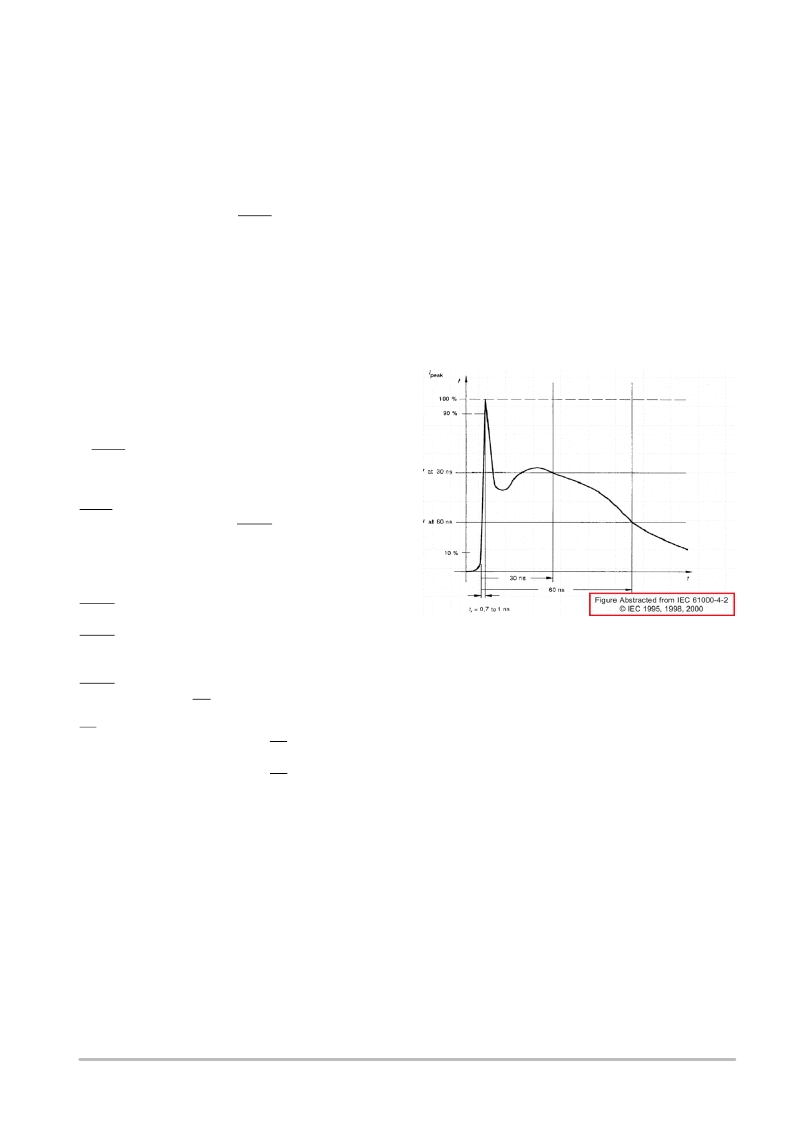
ESD Tests
The NCP348 input pin fully supports the IEC6100042.
1.0 F (minimum) must be connected between V
in
and
GND, close to the device.
That means, in Air condition, V
in
has a
protected input. In Contact condition, V
in
has
ESD protected input.
Please refer to Figure 19 to see the IEC 6100042
electrostatic discharge waveform.
15 kV ESD
8.0 kV
Figure 19. Electrostatic Discharge Waveform
PCB Recommendations
The NCP348 integrates a 2 amperes rated NMOS FET,
and the PCB rules must be respected to properly evacuate
the heat out of the silicon. The PAD1 is internally isolated
from the active silicon and should preferably be connected
to ground.
The PAD2 of the NCP348 package is connected
to the internal NMOS drain and can be used to increase the
heat transfer if necessary from an applications standpoint.
Depending upon the power dissipated in the application,
one can either use the PCB tracks connected to Pins 4 and
5 to evacuate heat, or make profit of the PAD2 area to add
extra copper surface to reduce the junction temperature
(See Figure 20).
Of course, in any case, this pad shall be not
connected to any other potential.
Figure 20 shows copper
area according to R
JA
and allows the design of the heat
transfer plane connected to PAD2.
相關(guān)PDF資料 |
PDF描述 |
|---|---|
| NCP400 | 150 mA CMOS Low Iq Low-Dropout Voltage Regulator with Voltage Detector Output |
| NCP400FCT2G | 150 mA CMOS Low Iq Low-Dropout Voltage Regulator with Voltage Detector Output |
| NCP4326DR2 | Secondary Controller for Multi−Output Quasi−Resonant Switchmode Power Supplies |
| NCP4326DR2G | Secondary Controller for Multi−Output Quasi−Resonant Switchmode Power Supplies |
| NCP4330DR2G | Post Regulation Driver |
相關(guān)代理商/技術(shù)參數(shù) |
參數(shù)描述 |
|---|---|
| NCP349 BB58C WAF | 制造商:ON Semiconductor 功能描述: |
| NCP349GEVB | 功能描述:電源管理IC開(kāi)發(fā)工具 POSITIVE OVP EVB RoHS:否 制造商:Maxim Integrated 產(chǎn)品:Evaluation Kits 類型:Battery Management 工具用于評(píng)估:MAX17710GB 輸入電壓: 輸出電壓:1.8 V |
| NCP349MNAETBG | 功能描述:電壓監(jiān)測(cè)器/監(jiān)控器 POSITIVE OVP RoHS:否 制造商:Texas Instruments 監(jiān)測(cè)電壓數(shù):2 監(jiān)測(cè)電壓:Adjustable 輸出類型:Open Drain 欠電壓閾值: 過(guò)電壓閾值: 準(zhǔn)確性:1 % 工作電源電壓:1.5 V to 6.5 V 工作電源電流:1.8 uA 最大工作溫度:+ 125 C 封裝 / 箱體:SON-6 安裝風(fēng)格:SMD/SMT |
| NCP349MNBGTBG | 功能描述:電壓監(jiān)測(cè)器/監(jiān)控器 POSITIVE OVP RoHS:否 制造商:Texas Instruments 監(jiān)測(cè)電壓數(shù):2 監(jiān)測(cè)電壓:Adjustable 輸出類型:Open Drain 欠電壓閾值: 過(guò)電壓閾值: 準(zhǔn)確性:1 % 工作電源電壓:1.5 V to 6.5 V 工作電源電流:1.8 uA 最大工作溫度:+ 125 C 封裝 / 箱體:SON-6 安裝風(fēng)格:SMD/SMT |
| NCP349MNBKTBG | 功能描述:電壓監(jiān)測(cè)器/監(jiān)控器 POSITIVE OVP RoHS:否 制造商:Texas Instruments 監(jiān)測(cè)電壓數(shù):2 監(jiān)測(cè)電壓:Adjustable 輸出類型:Open Drain 欠電壓閾值: 過(guò)電壓閾值: 準(zhǔn)確性:1 % 工作電源電壓:1.5 V to 6.5 V 工作電源電流:1.8 uA 最大工作溫度:+ 125 C 封裝 / 箱體:SON-6 安裝風(fēng)格:SMD/SMT |
發(fā)布緊急采購(gòu),3分鐘左右您將得到回復(fù)。